Datasheet Details
| Part number | CY2SSTV850 |
|---|---|
| Manufacturer | Cypress (now Infineon) |
| File Size | 152.68 KB |
| Description | Differential Clock Buffer/Driver |
| Datasheet |
 CY2SSTV850 Datasheet CY2SSTV850 Datasheet
|
|
|
| Part number | CY2SSTV850 |
|---|---|
| Manufacturer | Cypress (now Infineon) |
| File Size | 152.68 KB |
| Description | Differential Clock Buffer/Driver |
| Datasheet |
CY2SSTV850 Datasheet
|
|
|
|
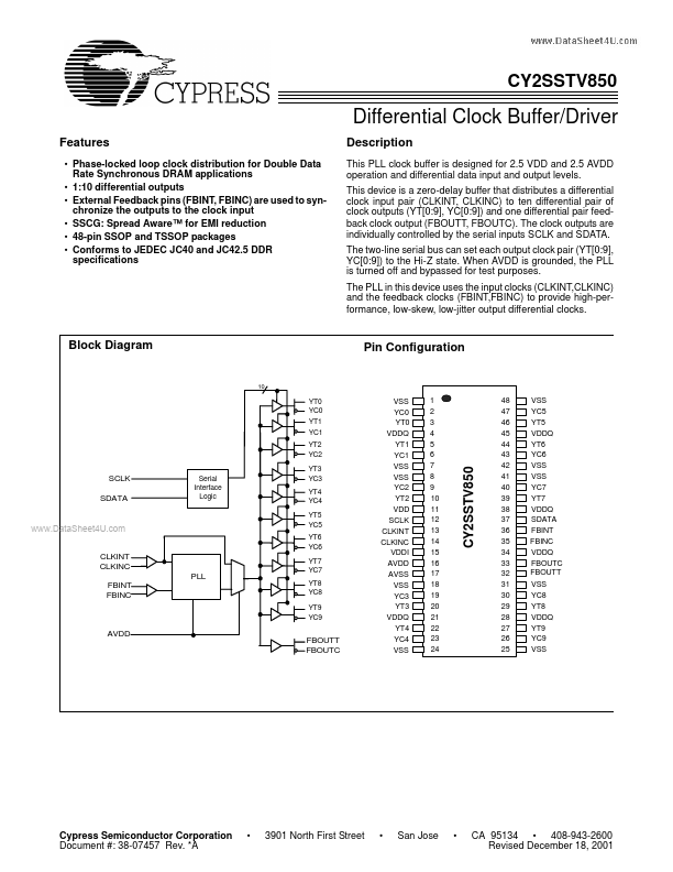
This PLL clock buffer is designed for 2.5 VDD and 2.5 AVDD operation and differential data input and output levels.
This device is a zero-delay buffer that distributes a differential clock input pair (CLKINT, CLKINC) to ten differential pair of clock outputs (YT[0:9], YC[0:9]) and one differential pair feedback clock output (FBOUTT, FBOUTC).
The clock outputs are individually controlled by the serial inputs SCLK and SDATA.
STV850 CY2SSTV850 Differential Clock Buffer/Driver.
| Brand Logo | Part Number | Description | Manufacturer |
|---|---|---|---|
| CY2SSTV850 | Differential Clock Buffer/Driver | Silicon Laboratories |
| Part Number | Description |
|---|---|
| CY2SSTV855 | Differential Clock Buffer/Driver |
| CY2SSTV857-27 | Differential Clock Buffer/Driver DDR333/PC2700-Compliant |
| CY2SSTV857-32 | Differential Clock Buffer/Driver DDR400/PC3200-Compliant |
| CY2SSTV8575 | Differential Clock Buffer/Driver |
| CY2SSTV16857 | 14-Bit Registered Buffer |
| CY2SSTV16859 | 13-Bit to 26-Bit Registered Buffer PC2700-/PC3200-Compliant |
| CY2SSTU877 | 10-Output JEDEC-Compliant Zero Delay Buffer |
| CY2037 | High Accuracy EPROM Programmable PLL Die for Crystal Oscillators |
| CY2071A | Single-PLL General-Purpose EPROM Programmable Clock Generator |
| CY2077 | High-accuracy EPROM Programmable Single-PLL Clock Generator |