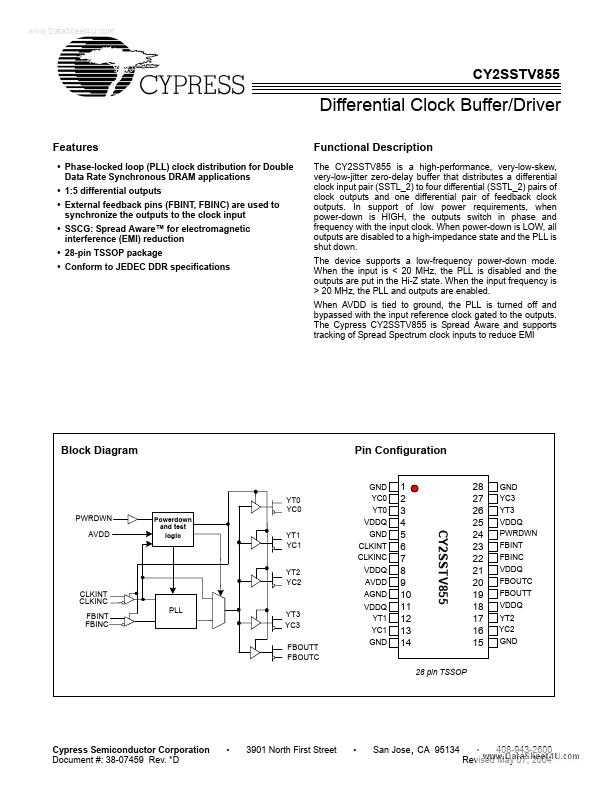
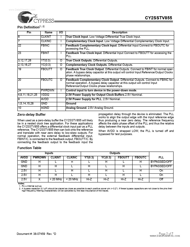
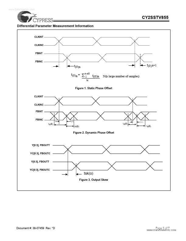
Datasheet4U Logo Datasheet4U.com

CY2SSTV855 - Differential Clock Buffer/Driver

General Description

The CY2SSTV855 is a high-performance, very-low-skew, very-low-jitter zero-delay buffer that distributes a differential clock input pair (SSTL_2) to four differential (SSTL_2) pairs of clock outputs and one differential pair of feedback clock outputs.

Key Features

  • Phase-locked loop (PLL) clock distribution for Double Data Rate Synchronous DRAM.

📥 Download Datasheet

Full PDF Text Transcription for CY2SSTV855 (Reference)

Note: Below is a high-fidelity text extraction (approx. 800 characters) for CY2SSTV855. For precise diagrams, and layout, please refer to the original PDF.

www.DataSheet4U.com CY2SSTV855 Differential Clock Buffer/Driver Features • Phase-locked loop (PLL) clock distribution for Double Data Rate Synchronous DRAM applications •...

View more extracted text
lock distribution for Double Data Rate Synchronous DRAM applications • 1:5 differential outputs • External feedback pins (FBINT, FBINC) are used to synchronize the outputs to the clock input • SSCG: Spread Aware™ for electromagnetic interference (EMI) reduction • 28-pin TSSOP package • Conform to JEDEC DDR specifications Functional Description The CY2SSTV855 is a high-performance, very-low-skew, very-low-jitter zero-delay buffer that distributes a differential clock input pair (SSTL_2) to four differential (SSTL_2) pairs of clock outputs and one differential pair of feedback clock outputs.