CY2SSTV855
Key Features
- Phase-locked loop (PLL) clock distribution for Double Data Rate Synchronous DRAM applications
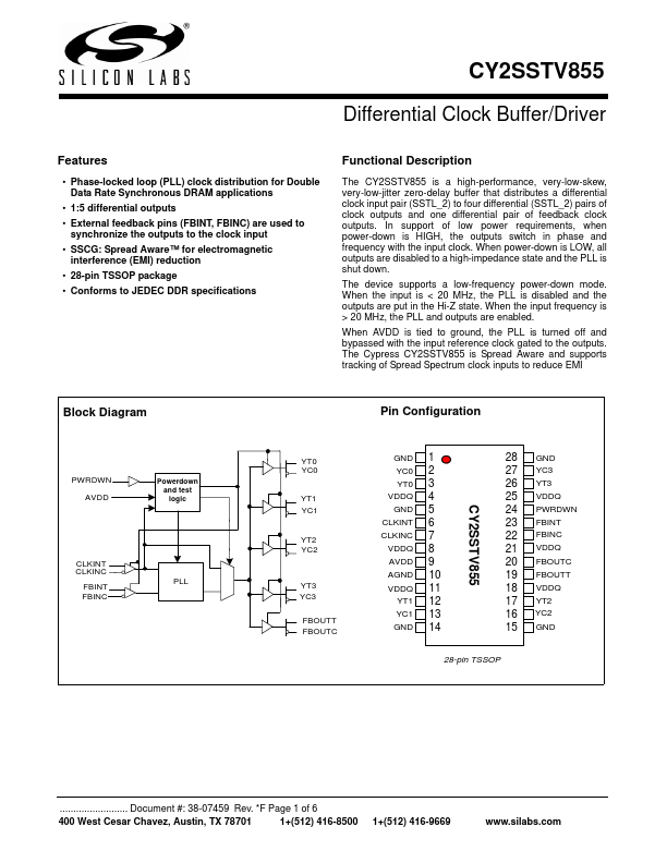
- 1:5 differential outputs
- External feedback pins (FBINT, FBINC) are used to synchronize the outputs to the clock input
- SSCG: Spread Aware™ for electromagnetic interference (EMI) reduction
- 28-pin TSSOP package
- Conforms to JEDEC DDR specifications