• Part: CY62157DV18
  • Description: 8M (512K x 16) Static RAM
  • Manufacturer: Cypress
  • Size: 158.36 KB
Download CY62157DV18 Datasheet PDF
Cypress
CY62157DV18
CY62157DV18 is 8M (512K x 16) Static RAM manufactured by Cypress.
Features - Very high speed: 55 ns and 70 ns - Voltage range: 1.65V to 1.95V - Pin patible with CY62157CV18 - Ultra-low active power - Typical active current: 1 m A @ f = 1 MHz - Typical active current: 10 m A @ f = f MAX - Ultra-low standby power - Easy memory expansion with CE1, CE2, and OE features - Automatic power-down when deselected - CMOS for optimum speed/power - 
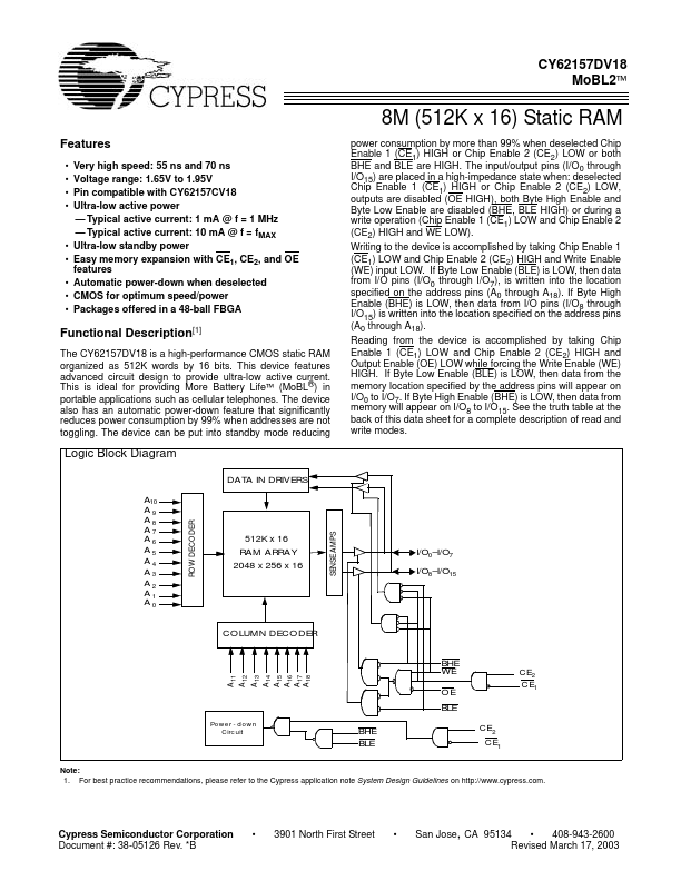
Packages offered in a 48-ball FBGA Functional Description [1] The CY62157DV18 is a high-performance CMOS static RAM organized as 512K words by 16 bits. This device features advanced circuit design to provide ultra-low active current. This is ideal for providing More Battery Life (Mo BL®) in portable applications such as cellular telephones. The device also has an automatic power-down feature that significantly reduces power consumption by 99% when addresses are not toggling. The device can be put into standby mode reducing Logic Block Diagram 8M (512K x 16) Static RAM power consumption by more than 99% when deselected Chip Enable 1 (CE1) HIGH or Chip Enable 2 (CE2) LOW or both BHE and BLE are HIGH. The input/output pins (I/O0 through I/O15) are placed in a high-impedance state when: deselected Chip Enable 1 (CE1) HIGH or Chip Enable 2 (CE2) LOW, outputs are disabled (OE HIGH), both Byte High Enable and Byte Low Enable are disabled (BHE, BLE HIGH) or during a write operation (Chip Enable 1 (CE1) LOW and Chip Enable 2 (CE2) HIGH and WE LOW). Writing to the device is acplished by taking Chip Enable 1 (CE1) LOW and Chip Enable 2 (CE2) HIGH and Write Enable (WE) input LOW. If Byte Low Enable (BLE) is LOW, then data from I/O pins (I/O0 through I/O7), is written into the location specified on the address pins (A0 through A18). If Byte High Enable (BHE) is LOW, then data from I/O pins (I/O8 through I/O15) is written into the location specified on the address pins (A0 through A18). Reading from the device is acplished by taking Chip Enable 1 (CE1) LOW and Chip Enable 2 (CE2) HIGH and Output Enable (OE) LOW...