Datasheet4U Logo Datasheet4U.com

CY7C1440AV33 - (CY7C144xAV33) Sync SRAM

Description

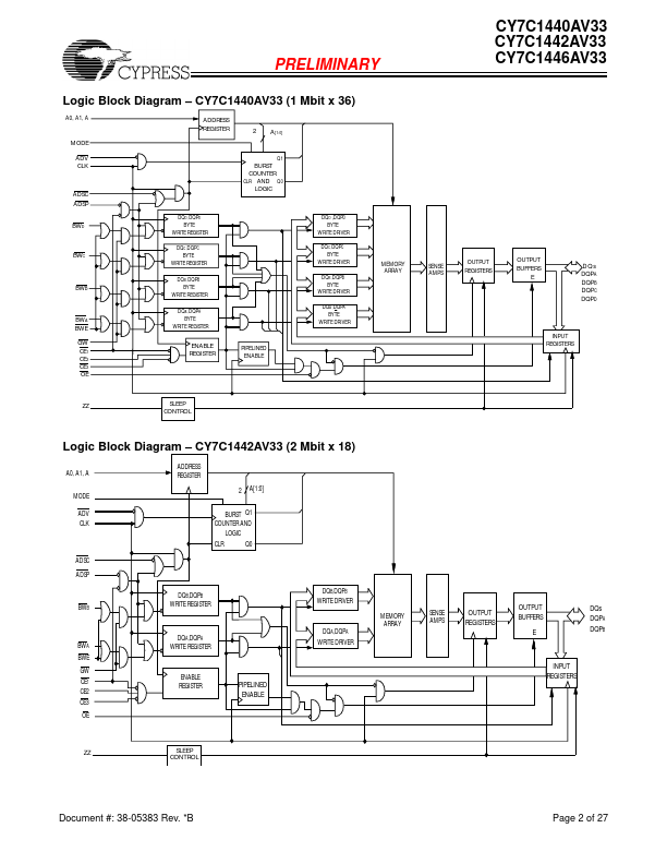
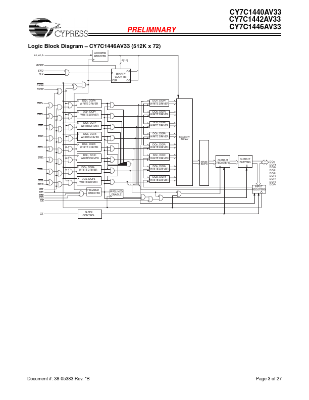
The CY7C1440AV33/CY7C1442AV33/CY7C1446AV33 SRAM integrates 1,048,576 x 36, 2,097,152 x 18 and 524,288 x 72 SRAM cells with advanced synchronous peripheral circuitry and a two-bit counter for internal burst operation.

Features

  • Supports bus operation up to 250 MHz.
  • Available speed grades are 250, 200,167 MHz.
  • Registered inputs and outputs for pipelined operation.
  • 3.3V core power supply.
  • 2.5V/3.3V I/O operation.
  • Fast clock-to-output times.
  • 2.6 ns (for 250-MHz device).
  • 3.2 ns (for 200-MHz device).
  • 3.4 ns (for 167-MHz device).
  • Provide high-performance 3-1-1-1 access rate.
  • User-selectable burst counter supporting Pentium® in.

📥 Download Datasheet

Full PDF Text Transcription (Reference)

The following content is an automatically extracted verbatim text from the original manufacturer datasheet and is provided for reference purposes only.

View original datasheet text
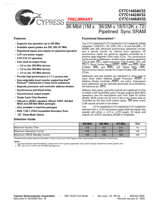
www.DataSheet4U.com PRELIMINARY CY7C1440AV33 CY7C1442AV33 CY7C1446AV33 36-Mbit (1M x 36/2M x 18/512K x 72) Pipelined Sync SRAM Features • Supports bus operation up to 250 MHz • Available speed grades are 250, 200,167 MHz • Registered inputs and outputs for pipelined operation • 3.3V core power supply • 2.5V/3.3V I/O operation • Fast clock-to-output times — 2.6 ns (for 250-MHz device) — 3.2 ns (for 200-MHz device) — 3.
Published: |