Datasheet Details
| Part number | CY7C1514AV18 |
|---|---|
| Manufacturer | Cypress (now Infineon) |
| File Size | 690.83 KB |
| Description | 72-Mbit QDR-II SRAM 2-Word Burst Architecture |
| Download | CY7C1514AV18 Download (PDF) |

|
|
Download the CY7C1514AV18 datasheet PDF. This datasheet also includes the CY7C1510AV18 variant, as both parts are published together in a single manufacturer document.
| Part number | CY7C1514AV18 |
|---|---|
| Manufacturer | Cypress (now Infineon) |
| File Size | 690.83 KB |
| Description | 72-Mbit QDR-II SRAM 2-Word Burst Architecture |
| Download | CY7C1514AV18 Download (PDF) |
|
|
|
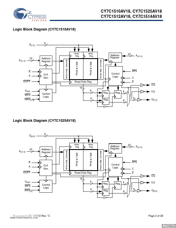
Maximum Operating Frequency Maximum Operating Current x8 x9 x18 x36 250 MHz 250 1230 1240 1350 1560 Configurations CY7C1510AV18 – 8M x 8 CY7C1525AV18 – 8M x 9 CY7C1512AV18 – 4M x 18 CY7C1514AV18 – 2M x 36 Functional Description The CY7C1510AV18, CY7C1525AV18, CY7C1512AV18, and CY7C1514AV18 are 1.8V Synchronous Pipelined SRAMs, equipped with QDR™-II architecture.
QDR-II architecture consists of two separate ports: the read port and the write port to access the memory array.
The read port has dedicated data outputs to support read operations and the write port has dedicated data inputs to support
CY7C1510AV18, CwYww7.DCat1a5Sh2ee5t4AU.Vco1m8 CY7C1512AV18, CY7C1514AV18 72-Mbit QDR™-II SRAM 2-Word Burst.
| Part Number | Description |
|---|---|
| CY7C1514KV18 | 72-Mbit QDR II SRAM Two-Word Burst Architecture |
| CY7C1514V18 | 1.8V Synchronous Pipelined SRAM |
| CY7C1510AV18 | 72-Mbit QDR-II SRAM 2-Word Burst Architecture |
| CY7C1510V18 | 1.8V Synchronous Pipelined SRAM |
| CY7C1511AV18 | 72-Mbit QDR-II SRAM 4-Word Burst Architecture |
| CY7C1511JV18 | 72-Mbit QDR-II SRAM 4-Word Burst Architecture |
| CY7C1511KV18 | (CY7C15xxKV18) 72-Mbit QDR II SRAM 4-Word Burst Architecture |
| CY7C1511V18 | (CY7C15xxV18) SRAM 4-Word Burst Architecture |
| CY7C1512 | 64K x 8 Static RAM |
| CY7C1512AV18 | 72-Mbit QDR-II SRAM 2-Word Burst Architecture |