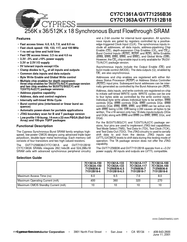
Datasheet4U Logo Datasheet4U.com

GVT71512B18 - 256K x 36 / 512K x 18 Sunchronous Burse Flowthrough SRAM

Download the GVT71512B18 datasheet PDF. This datasheet also covers the GVT71256B36 variant, as both devices belong to the same 256k x 36 / 512k x 18 sunchronous burse flowthrough sram family and are provided as variant models within a single manufacturer datasheet.

Description

The Cypress Synchronous Burst SRAM family employs highspeed, low-power CMOS designs using advanced triple-layer polysilicon, double-layer metal technology.

Each memory cell consists of four transistors and two high-valued resistors.

Features

  • Fast access times: 6.0, 6.5, 7.0, and 8.0 ns Fast clock speed: 150, 133, 117, and 100 MHz 1 ns set-up time and hold time Fast OE access times: 3.5 ns and 4.0 ns 3.3V.
  • 5% and +10% power supply 3.3V or 2.5V I/O supply 5V tolerant inputs except I/Os Clamp diodes to VSS at all inputs and outputs Common data inputs and data outputs Byte Write Enable and Global Write control Multiple c.

📥 Download Datasheet

Note: The manufacturer provides a single datasheet file (GVT71256B36_CypressSemiconductor.pdf) that lists specifications for multiple related part numbers.

Full PDF Text Transcription (Reference)

The following content is an automatically extracted verbatim text from the original manufacturer datasheet and is provided for reference purposes only.

View original datasheet text
( DataSheet : www.DataSheet4U.com ) 1CY7C1361A CY7C1361A/GVT71256B36 CY7C1363A/GVT71512B18 256K x 36/512K x 18 Synchronous Burst Flowthrough SRAM Features • • • • • • • • • • • Fast access times: 6.0, 6.5, 7.0, and 8.0 ns Fast clock speed: 150, 133, 117, and 100 MHz 1 ns set-up time and hold time Fast OE access times: 3.5 ns and 4.0 ns 3.3V –5% and +10% power supply 3.3V or 2.
Datasheet originally released: |