W40S11-23
W40S11-23 is Clock Buffer/Driver manufactured by Cypress.
Clock Buffer/Driver
Features
- Thirteen skew-controlled CMOS clock outputs (SDRAM0:12)
- Supports three SDRAM DIMMs
- Ideal for high-performance systems designed around Intel’s latest chip set
- I2C serial configuration interface
- Clock Skew between any two outputs is less than 250 ps
- 1- to 5-ns propagation delay
- DC to 133-MHz operation
- Single 3.3V supply voltage
- Low power CMOS design packaged in a 28-pin, 300-mil SOIC (Small Outline Integrated Circuit)
Key Specifications
Supply Voltages:........................................... VDD = 3.3V±5% Operating Temperature:.................................... 0°C to +70°C Input Threshold: .................................................. 1.5V typical Maximum Input Voltage: .......................................VDD + 0.5V Input Frequency:............................................... 0 to 133 MHz BUF_IN to SDRAM0:12 Propagation Delay: ...... 1.0 to 5.0 ns Output Edge Rate:.............................................. >1.5 V/ns Output Clock Skew: .................................................. ±250 ps Output Duty Cycle: .................................. 45/55% worst case Output Impedance: ...............................................15Ω typical Output Type: ................................................ CMOS rail-to-rail
Overview
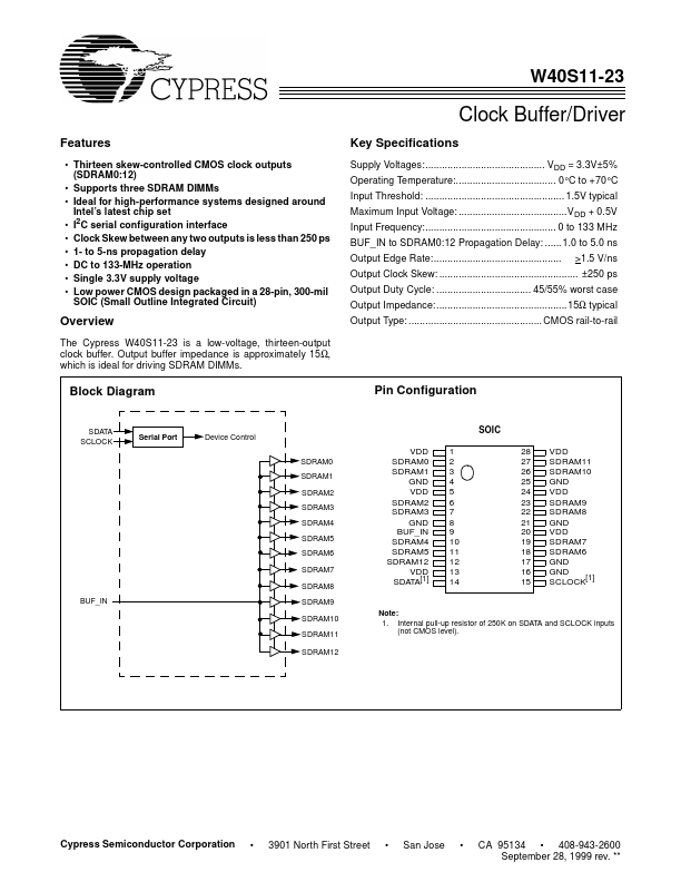
The Cypress W40S11-23 is a low-voltage, thirteen-output clock buffer. Output buffer impedance is approximately 15Ω, which is ideal for driving SDRAM DIMMs.
Block Diagram
Pin Configuration
SDATA SCLOCK
Serial Port
Device Control SDRAM0 SDRAM1 SDRAM2 SDRAM3 SDRAM4 SDRAM5 SDRAM6 SDRAM7 SDRAM8
SOIC VDD SDRAM0 SDRAM1 GND VDD SDRAM2 SDRAM3 GND BUF_IN SDRAM4 SDRAM5 SDRAM12 VDD SDATA[1] 1 2 3 4 5 6 7 8 9 10 11 12 13 14 28 27 26 25 24 23 22 21 20 19 18 17 16 15 VDD SDRAM11 SDRAM10 GND VDD SDRAM9 SDRAM8 GND VDD SDRAM7 SDRAM6 GND GND [1] SCLOCK
BUF_IN
SDRAM9 SDRAM10 SDRAM11 SDRAM12 Note: 1. Internal pull-up resistor of 250K on SDATA and SCLOCK inputs (not CMOS...


