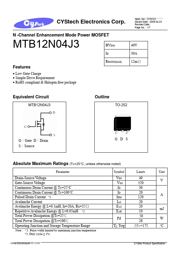
MTB12N04J3
MTB12N04J3 is N -Channel Enhancement Mode Power MOSFET manufactured by Cystech Electonics.
Features
- Low Gate Charge
- Simple Drive Requirement
- Ro HS pliant & Halogen-free package
BVDSS ID RDSON(MAX)
40V 30A 12mΩ
Equivalent Circuit
Outline
TO-252
G:Gate D:Drain S:Source
Absolute Maximum Ratings (TC=25°C, unless otherwise noted)
Parameter Symbol Limits Unit
Drain-Source Voltage Gate-Source Voltage Continuous Drain Current @ TC=25°C Continuous Drain Current @ TC=100°C Pulsed Drain Current
- 1 Avalanche Current Avalanche Energy @ L=0.1m H, ID=20A, RG=25Ω Repetitive Avalanche Energy @ L=0.05m H
- 2 Total Power Dissipation @TC=25℃ Total Power Dissipation @TC=100℃ Operating Junction and Storage Temperature Range Note :
- 1. Pulse width limited by maximum junction temperature
- 2. Duty cycle ≤ 1%
VDS VGS ID ID IDM IAS EAS EAR Pd Tj, Tstg
40 ±20 30 20 120 20 20 10 50 26 -55~+175
A m J W °C
CYStek Product Specification
CYStech Electronics Corp.
Thermal Data
Parameter Thermal Resistance, Junction-to-case, max Thermal Resistance, Junction-to-ambient, max Symbol Rth,j-c Rth,j-a
.. Spec. No. : C707J3 Issued Date : 2009.04.23 Revised Date : Page No. : 2/7
Value 3 75
Unit °C/W °C/W
Characteristics (Tc=25°C, unless otherwise specified)
Symbol Static BVDSS VGS(th) GFS IGSS IDSS ID(ON) RDS(ON)
- 1
- 1
Min. 40 1.5 30
- Typ. 1.8 25 10.8 15.5 22 3.6 7 3 11 16 6 1700 180 106 2 60 42
Max. 3.2 ±100 1 25 12 20 25 100 1.3
- Unit V V S n A μA μA A mΩ mΩ
Test Conditions VGS=0, ID=250μA VDS =VGS, ID=250μA VDS =5V, ID=20A VGS=±20, VDS=0 VDS =32V, VGS =0 VDS =30V, VGS =0, Tj=125°C VDS =10V, VGS =10V VGS =10V, ID=20A VGS =7V, ID=15A
- 1
Dynamic...