PI6CBE33123
Key Features
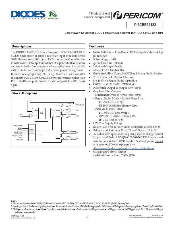
- It takes a reference input to fanout twelve 100MHz low-power differential HCSL outputs with on-chip terminations for 33Ω output impedance
- It supports both zero-delay and fanout buffer functions for various applications
- An individual OE pin for each output provides easier power management
- It uses Diodes proprietary PLL design to achieve very-low jitter that meets PCIe 1.0/2.0/3.0/4.0/5.0/6.0 requirements
- Other than PCIe 100MHz support, this device also supports 133.33MHz via a pin