DMC2990UDJ
DMC2990UDJ is MOSFET manufactured by Diodes Incorporated.
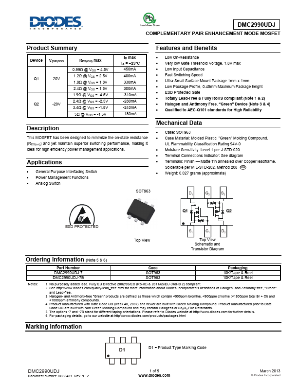
AADNDVEVAAWNNPCNCEREE IOWIDNNPFUFROCOORTRDMMUAACTTITIOONN
PLEMENTARY PAIR ENHANCEMENT MODE MOSFET
Product Summary
Features and Benefits
Device V(BR)DSS Q1 20V
Q2 -20V
RDS(ON) max
0.99Ω @ VGS = 4.5V 1.2Ω @ VGS = 2.5V 1.8Ω @ VGS = 1.8V 2.4Ω @ VGS = 1.5V 1.9Ω @ VGS = -4.5V 2.4Ω @ VGS = -2.5V 3.4Ω @ VGS = -1.8V 5Ω @ VGS = -1.5V
ID max TA = +25°C
450mA 400mA 330mA 300mA -310mA -280mA -240mA -180mA
Description
This MOSFET has been designed to minimize the on-state resistance (RDS(on)) and yet maintain superior switching performance, making it ideal for high efficiency power management applications.
Applications
- General Purpose Interfacing Switch
- Power Management...