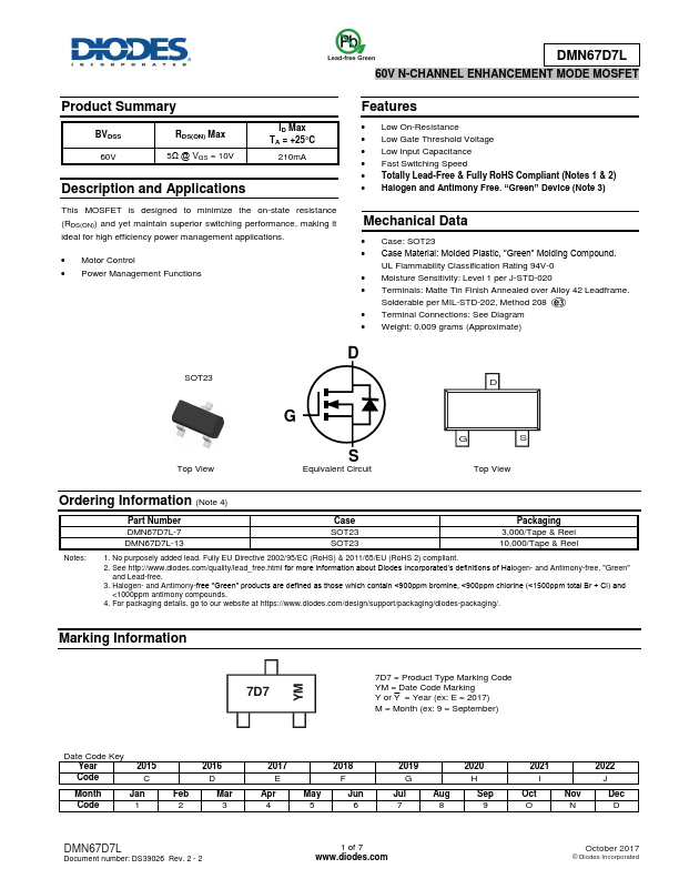
Maximum Ratings (@TA = +25°C, unless otherwise specified.)
Characteristic
Drain-Source Voltage
Gate-Source Voltage
Continuous Drain Current (Note 6) VGS = 10V
Steady
State
Maximum Body Diode Forward Current (Note 6)
Pulsed Drain Current (10µs Pulse, Duty Cycle = 1%)
TA = +25°C
TA = +85°C
Symbol
VDSS
VGSS
ID
IS
IDM
DMN67D7L
Value
60
±40
210
150
500
800
Unit
V
V
mA
mA
mA
Thermal Characteristics (@TA = +25°C, unless otherwise specified.)
Characteristic
Total Power Dissipation (Note 5)
Thermal Resistance, Junction to Ambient (Note 5)
Total Power Dissipation (Note 6)
Thermal Resistance, Junction to Ambient (Note 6)
Operating and Storage Temperature Range
Steady State
Steady State
Symbol
PD
RθJA
PD
RθJA
TJ, TSTG
Value
340
376
570
224
-55 to +150
Unit
mW
°C/W
mW
°C/W
°C
Electrical Characteristics (@TA = +25°C, unless otherwise specified.)
Characteristic
OFF CHARACTERISTICS (Note 7)
Drain-Source Breakdown Voltage
Zero Gate Voltage Drain Current
Gate-Source Leakage
ON CHARACTERISTICS (Note 7)
Gate Threshold Voltage
Symbol
BVDSS
IDSS
IGSS
VGS(TH)
Min
60
0.8
Static Drain-Source On-Resistance
RDS(ON)
Diode Forward Voltage
DYNAMIC CHARACTERISTICS (Note 8)
Input Capacitance
Output Capacitance
Reverse Transfer Capacitance
Gate Resistance
Total Gate Charge (VGS = 4.5V)
Total Gate Charge (VGS = 10V)
Gate-Source Charge
Gate-Drain Charge
Turn-On Delay Time
Turn-On Rise Time
Turn-Off Delay Time
Turn-Off Fall Time
VSD
Ciss
Coss
Crss
Rg
Qg
Qg
Qgs
Qgd
tD(ON)
tR
tD(OFF)
tF
Notes:
5. Device mounted on FR-4 PCB, with minimum recommended pad layout.
6. Device mounted on 1” x 1” FR-4 PCB with high coverage 2oz. Copper, single sided.
7. Short duration pulse test used to minimize self-heating effect.
8. Guaranteed by design. Not subject to product testing.
Typ
3.2
1.5
0.78
22
4.1
2.5
120
361
821
162
116
2.8
3.0
7.6
5.6
Max Unit
Test Condition
1.0
±100
V VGS = 0V, ID = 10µA
µA VDS = 60V, VGS = 0V
nA VGS = ±20V, VDS = 0V
2.5 V VDS = VGS, ID = 250µA
7.5
5.0
VGS = 5.0V, ID = 0.05A
VGS = 10V, ID = 0.5A
1.5 V VGS = 0V, IS = 115mA
pF
pF
VDS = 25V, VGS = 0V,
f = 1.0MHz
pF
VDS = 0V, VGS = 0V, f = 1.0MHz
pC VDS = 10V, ID = 250mA
VDD = 30V, ID = 0.2A,
ns RL = 150, VGEN = 10V,
RGEN = 25
DMN67D7L
Document number: DS39026 Rev. 2 - 2
2 of 7
www.diodes.com
October 2017
© Diodes Incorporated