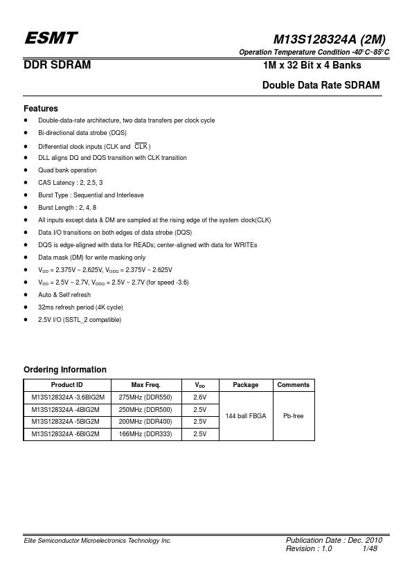
M13S128324A
M13S128324A is Double Data Rate SDRAM manufactured by Elite Semiconductor Microelectronics Technology.
ESMT
DDR SDRAM
M13S128324A (2M)
Operation Temperature Condition -40°C~85°C
1M x 32 Bit x 4 Banks
Double Data Rate SDRAM
Features
- Double-data-rate architecture, two data transfers per clock cycle
- Bi-directional data strobe (DQS)
- Differential clock inputs (CLK and CLK )
- DLL aligns DQ and DQS transition with CLK transition
- Quad bank operation
- CAS Latency : 2, 2.5, 3
- Burst Type : Sequential and Interleave
- Burst Length : 2, 4, 8
- All inputs except data & DM are sampled at the rising edge of the system clock(CLK)
- Data I/O transitions on both edges of data strobe (DQS)
- DQS is edge-aligned with data for READs; center-aligned with data for WRITEs
- Data mask (DM) for write...