Part number:
M14F5121632A
Manufacturer:
ESMT
File Size:
1.95 MB
Description:
Ddr ii sdram.
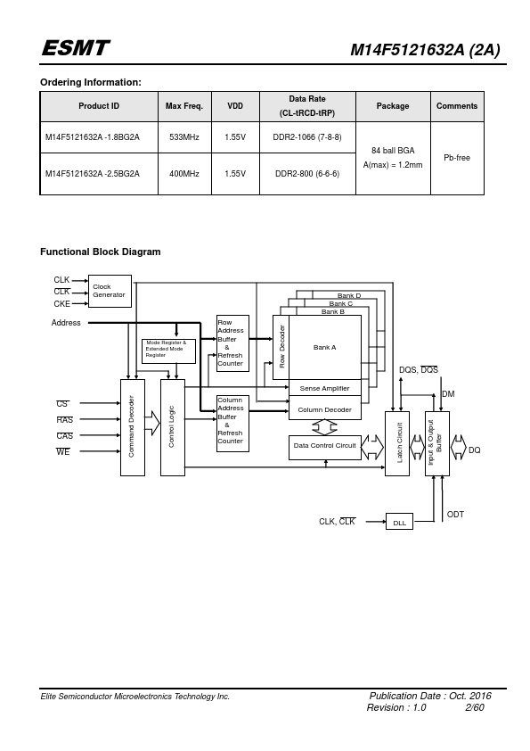
M14F5121632A Features
* JEDEC Standard
* VDD / VDDQ = 1.55V ± 0.075V
* Internal pipelined double-data-rate architecture; two data access per clock cycle
* Bi-directional differential data strobe (DQS, DQS ); DQS can be disabled for single-ended data strobe operation.
* On-chip DLL
* Differential c
M14F5121632A Datasheet (1.95 MB)
Datasheet Details
M14F5121632A
ESMT
1.95 MB
Ddr ii sdram.
📁 Related Datasheet
M140NWR1-R0 TFT LCD (IVO)
M140NWR2-R0 TFT LCD (IVO)
M140NWR2-R1 TFT LCD (IVO)
M140NWR2-R2 TFT LCD (IVO)
M141-X76C TFT Color LCD (IMES)
M141-X76H TFT Color LCD (IMES)
M141NWW1-101 TFT LCD (MTDis)
M141NWW1-103 TFT LCD Module (IVO)
TAGS
M14F5121632A Distributor