EMB9930G Description
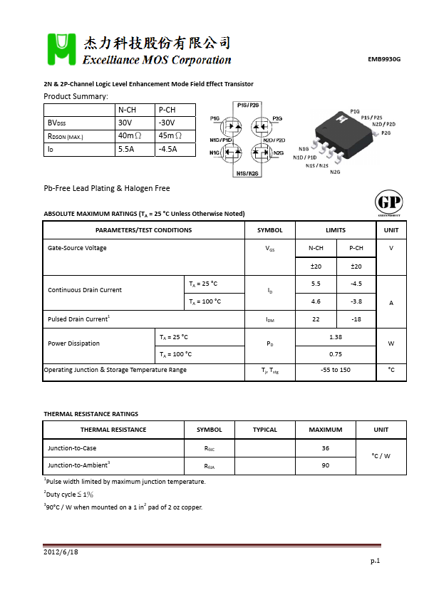
2N & 2P‐Channel Logic Level Enhancement Mode Field Effect Transistor Product Summary: 2Duty cycle 1% 390°C / W when mounted on a 1 in2 pad of 2 oz copper. Pulse Width 300 sec, Duty Cycle 2%.
EMB9930G is 2N & 2P-Channel Logic Level Enhancement Mode Field Effect Transistor manufactured by Excelliance MOS.
| Part Number | Description |
|---|---|
| EMB99A0G | MOSFET |
| EMB90A08G | MOSFET |
| EMB90N08A | N-Channel Logic Level Enhancement Mode Field Effect Transistor |
| EMB90N08G | MOSFET |
| EMB90N08V | MOSFET |
2N & 2P‐Channel Logic Level Enhancement Mode Field Effect Transistor Product Summary: 2Duty cycle 1% 390°C / W when mounted on a 1 in2 pad of 2 oz copper. Pulse Width 300 sec, Duty Cycle 2%.