• Part: 74F194
  • Description: 4-Bit Bidirectional Universal Shift Register
  • Manufacturer: Fairchild Semiconductor
  • Size: 76.97 KB
Download 74F194 Datasheet PDF
Fairchild Semiconductor
74F194
74F194 is 4-Bit Bidirectional Universal Shift Register manufactured by Fairchild Semiconductor.
Description 
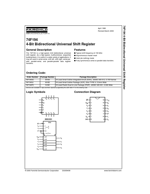
The 74F194 is a high-speed 4-bit bidirectional universal shift register. As a high-speed, multifunctional, sequential building block, it is useful in a wide variety of applications. It may be used in serial-serial, shift left, shift right, serial-parallel, parallel-serial, and parallel-parallel data register transfers. Features s Typical shift frequency of 150 MHz s Asynchronous master reset s Hold (do nothing) mode s Fully synchronous serial or parallel data transfers Ordering Code: Order Number 74F194SC 74F194SJ 74F194PC Package Number M16A M16D N16E Package Description 16-Lead Small Outline Integrated Circuit (SOIC), JEDEC MS-012, 0.150 Narrow 16-Lead Small Outline Package (SOP), EIAJ TYPE II, 5.3mm Wide 16-Lead Plastic Dual-In-Line Package (PDIP), JEDEC MS-001, 0.300 Wide Devices also available in Tape and Reel. Specify by appending the suffix letter “X” to the ordering code. Logic Symbols Connection Diagram IEEE/IEC © 2000 Fairchild Semiconductor Corporation DS009498 .fairchildsemi. Unit Loading/Fan Out Pin Names S0 , S1 P0- P3 DSR DSL CP MR Q0- Q3 Description Mode Control Inputs Parallel Data Inputs Serial Data Input (Shift Right) Serial Data Input (Shift Left) Clock Pulse Input (Active Rising Edge) Asynchronous Master Reset Input (Active LOW) Parallel Outputs U.L. HIGH/LOW 1.0/1.0 1.0/1.0 1.0/1.0 1.0/1.0 1.0/1.0 1.0/1.0 50/33.3 Input IIH/IIL Output IOH/IOL 20 µA/- 0.6 m A 20 µA/- 0.6 m A 20 µA/- 0.6 m A 20 µA/- 0.6 m A 20 µA/- 0.6 m A 20 µA/- 0.6 m A - 1 m A/20 m A Functional Description The 74F194 contains four edge-triggered D-type flip-flops and the necessary interstage logic to synchronously perform shift right, shift left, parallel load and hold operations. Signals applied to the Select (S0, S1) inputs determine the type of operation, as shown in the Mode Select Table. Signals on the Select, Parallel data (P0- P3) and Serial data (DSR, DSL) inputs can change when the clock is in either state, provided only that the remended setup and hold...