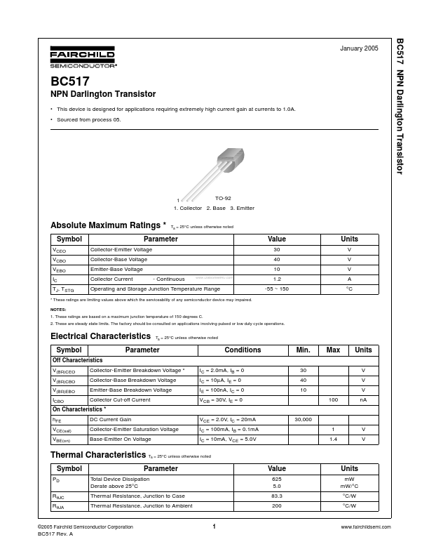
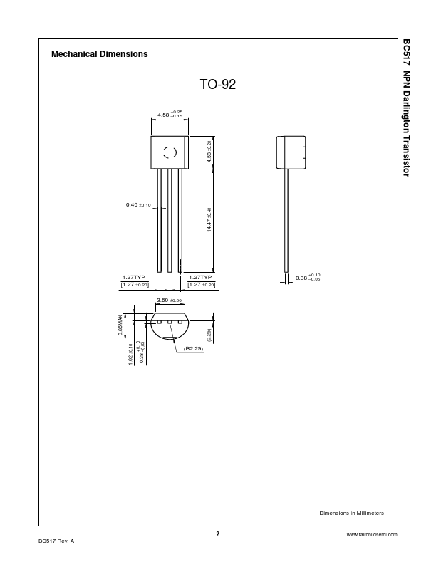
The following content is an automatically extracted verbatim text
from the original manufacturer datasheet and is provided for reference purposes only.
View original datasheet text
BC517 NPN Darlington Transistor
January 2005
BC517
NPN Darlington Transistor
• This device is designed for applications requiring extremely high current gain at currents to 1.0A. • Sourced from process 05.
1
TO-92
1. Collector 2. Base 3. Emitter
Absolute Maximum Ratings *
Symbol
VCEO VCBO VEBO IC TJ, TSTG Collector-Emitter Voltage Collector-Base Voltage Emitter-Base Voltage Collector Current
Ta = 25°C unless otherwise noted
Parameter
Value
30 40 10
www.DataSheet4U.com
Units
V V V A °C
- Continuous
1.2 -55 ~ 150
Operating and Storage Junction Temperature Range
* These ratings are limiting values above which the serviceability of any semiconductor device may impaired. NOTES: 1. These ratings are based on a maximum junction temperature of 150 degrees C. 2.