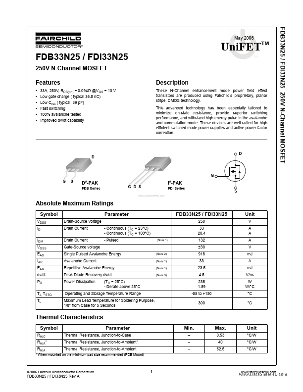
FDB33N25 Key Features
- 33A, 250V, RDS(on) = 0.094Ω @VGS = 10 V
- Low gate charge ( typical 36.8 nC)
- Low Crss ( typical 39 pF)
- Fast switching
- 100% avalanche tested
- Improved dv/dt capability
FDB33N25 is N-Channel MOSFET manufactured by Fairchild.
| Manufacturer | Part Number | Description |
|---|---|---|
| FDB33N25 | N-Channel MOSFET |
May 2006 TM These N-Channel enhancement mode power field effect transistors are produced using Fairchild’s proprietary, planar stripe, DMOS technology. This advanced technology has been especially tailored to minimize on-state resistance, provide superior switching performance, and withstand high energy pulse in the avalanche and mutation mode. These devices are well suited for high efficient switched mode power...