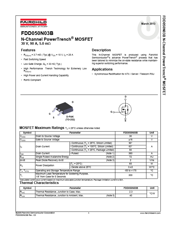
Datasheet Details
| Part number | FDD050N03B |
|---|---|
| Manufacturer | Fairchild (now onsemi) |
| File Size | 435.12 KB |
| Description | N-Channel PowerTrench MOSFET |
| Datasheet |
|
|
|
|
| Part number | FDD050N03B |
|---|---|
| Manufacturer | Fairchild (now onsemi) |
| File Size | 435.12 KB |
| Description | N-Channel PowerTrench MOSFET |
| Datasheet |
|
|
|
|
This N-Channel MOSFET is produced using Fairchild Semiconductor®’s advance PowerTrench® process that has been tailored to minimize the on-state resistance while maintaining superior switching performance.
Applications • Synchronous Rectification for ATX / Server / Telecom PSU D D G S D-PAK (TO-252) G S MOSFET Maximum Ratings TC = 25oC unless otherwise noted Symbol Parameter FDD050N03B VDSS VGSS ID IDM EAS dv/dt PD Drain to Source Voltage Gate to Source Voltage Drain Current Drain Current - Continuous (TC = 25oC, Silicon Limited) - Continuous (TC = 100oC, Silicon Limited) - Continuous (TC = 25oC, Package Limited) - Pulsed (Note 1) Single Pulsed Avalanche Energy (Note 2) Peak Diode Recovery dv/dt Power Dissipation (TC = 25oC) - Derate above 25oC (Note 3) 30 ±16 90* 63* 50 360 72 2 65 0.43 TJ, TSTG TL Operating and Storage Temperature Range Maximum Lead Temperature for Soldering Purpose, 1/8” from Case for 5 Seconds -55 to +175 300 *Calculated continuous current based on maximum allowable junction temperature.
Package limitation current is 50A.
FDD050N03B N-Channel PowerTrench® MOSFET March 2013 FDD050N03B N-Channel PowerTrench® MOSFET 30 V, 90 A, 5.
| Part Number | Description |
|---|---|
| FDD044AN03L | N-Channel PowerTrench MOSFET |
| FDD068AN03L | N-Channel MOSFET |
| FDD107AN06LA0 | N-Channel PowerTrench MOSFET |
| FDD10AN06A0 | N-Channel MOSFET |
| FDD10AN06A0_F085 | MOSFET |
| FDD10N20LZ | MOSFET |
| FDD120AN15A0 | N-Channel PowerTrench MOSFET |
| FDD13AN06A0 | N-Channel PowerTrench MOSFET |
| FDD14AN06LA0 | N-Channel PowerTrench MOSFET |
| FDD14AN06LA0_F085 | N-Channel PowerTrench MOSFET |