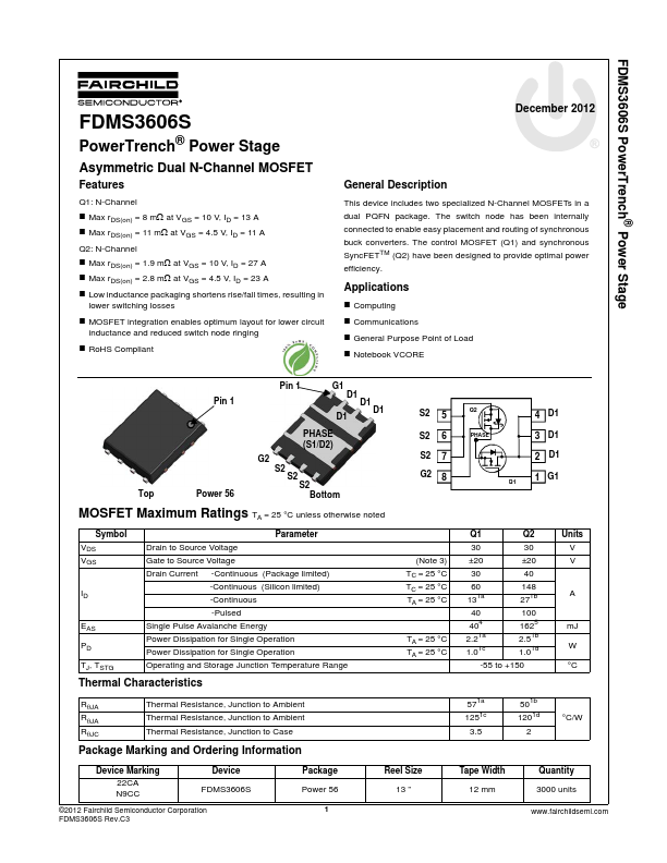
FDMS3606S Overview
This device includes two specialized N-Channel MOSFETs in a dual PQFN package. The switch node has been internally connected to enable easy placement and routing of synchronous buck converters. The control MOSFET (Q1) and synchronous SyncFETTM (Q2) have been designed to provide optimal power efficiency.
FDMS3606S Key Features
- Max rDS(on) = 8 mΩ at VGS = 10 V, ID = 13 A
- Max rDS(on) = 11 mΩ at VGS = 4.5 V, ID = 11 A
- Max rDS(on) = 1.9 mΩ at VGS = 10 V, ID = 27 A
- Max rDS(on) = 2.8 mΩ at VGS = 4.5 V, ID = 23 A
- MOSFET integration enables optimum layout for lower circuit inductance and reduced switch node ringing
- RoHS pliant
FDMS3606S Applications
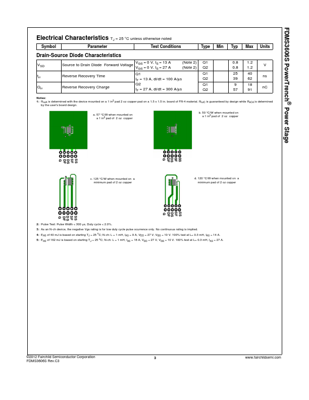
- Continuous (Silicon limited) -Continuous -Pulsed Single Pulse Avalanche Energy Power Dissipation for Single Operation Power Dissipation for Single Operation Ope