FDMS86520L
Overview
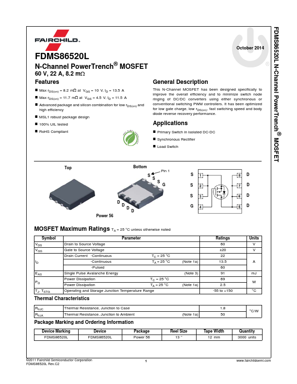
Max rDS(on) = 8.2 mΩ at VGS = 10 V, ID = 13.5 A Max rDS(on) = 11.7 mΩ at VGS = 4.5 V, ID = 11.5 A Advanced package and silicon combination for low rDS(on) and high efficiency MSL1 robust package design 100% UIL tested This N-Channel MOSFET has been designed specifically to improve the overall efficiency and to minimize switch node ringing of DC/DC converters using either synchronous or conventional switching PWM controllers. It has been optimized for low gate charge, low rDS(on), fast switching speed and body diode reverse recovery performance.