FQD3N60 Overview
Key Specifications
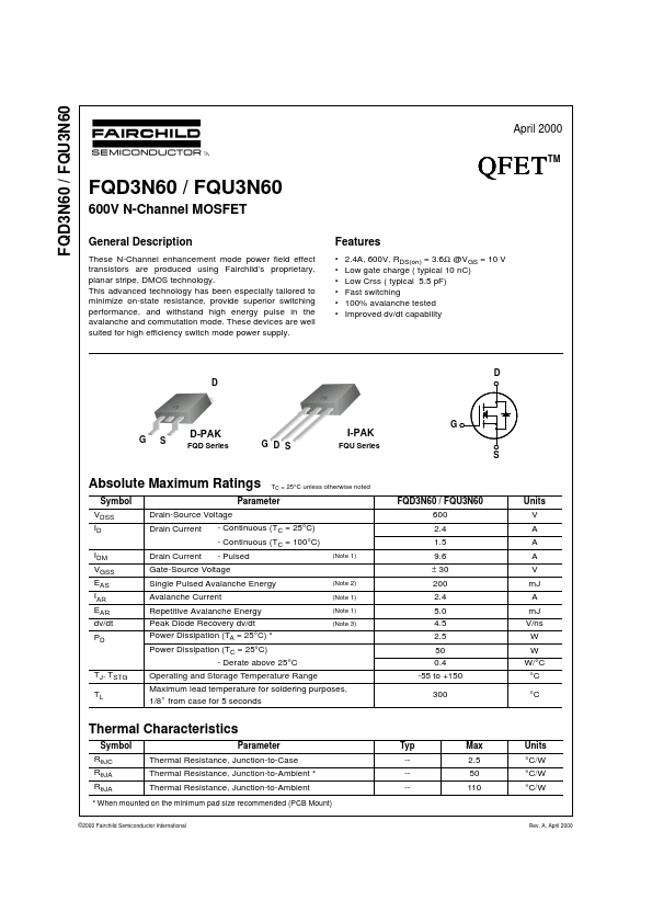
Package: DPAK
Mount Type: Surface Mount
Pins: 3
Height: 2.517 mm
Description
These N-Channel enhancement mode power field effect transistors are produced using Fairchild’s proprietary, planar stripe, DMOS technology. This advanced technology has been especially tailored to minimize on-state resistance, provide superior switching performance, and withstand high energy pulse in the avalanche and commutation mode.
Key Features
- " " " D-PAK FQD Series I-PAK G D S FQU Series !