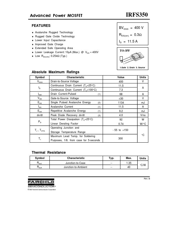
Low RDS(ON): 0.254Ω (Typ. )
Absolute Maximum Ratings
Symbol VDSS
ID
IDM VGS EAS IAR EAR dv/dt
PD
TJ , TSTG
TL
Characteristic
Drain-to-Source Voltage
Continuous Drain Current (TC=25°C)
Continuous Drain Current (TC=100°C)
Drain Current-Pulsed
(1).
Full PDF Text Transcription for IRFS350 (Reference)
Note: Below is a high-fidelity text extraction (approx. 800 characters) for
IRFS350. For precise diagrams, and layout, please refer to the original PDF.
Input Capacitance ♦ Improved Gate Charge ♦ Extended Safe Operating Area ♦ Lower Leakage Current: 10µA (Max.) @ VDS = 400V ♦ Low RDS(ON): 0.254Ω (Typ.) Absolute Maximum Ratings Symbol VDSS ID IDM VGS EAS IAR EAR dv/dt PD TJ , TSTG TL Characteristic Drain-to-Source Voltage Continuous Drain Current (TC=25°C) Continuous Drain Current (TC=100°C) Drain Current-Pulsed (1) Gate-to-Source Voltage Single Pulsed Avalanche Energy (2) Avalanche Current (1) Repetitive Avalanche Energy (1) Peak Diode Recovery dv/dt (3) Total Power Dissipation (TC=25°C) Linear Derating Factor Operating Junction and Storage Temperature Range Maximum Lead T