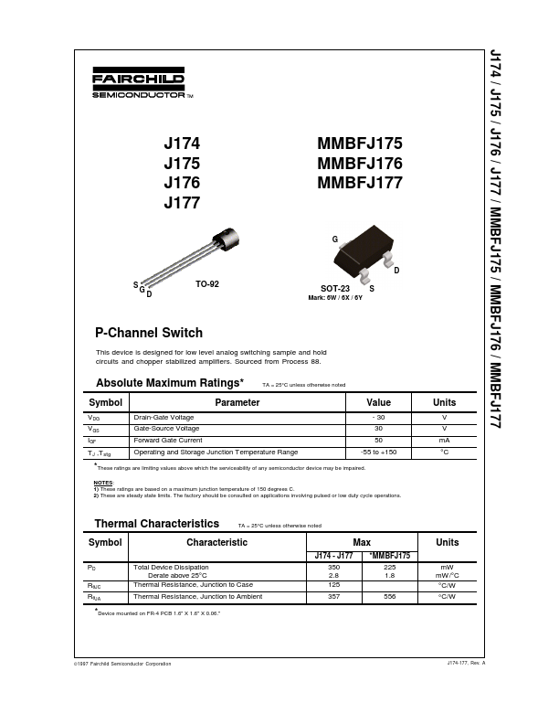
J175 Overview
Key Features
- 30 30 50 -55 to +150
- 10 nA J174 J175 J176 J177 5.0 3.0 1.0 0.8 30 1.0 10 6.0 4.0 2.5 V nA V V V V
| Part | J175 |
|---|---|
| Description | P-Channel Switch |
| Manufacturer | Fairchild Semiconductor |
| Size | 58.40 KB |
| Part Number | Manufacturer | Description |
|---|---|---|
| J175 | InterFET | P-Channel JFET |
| J175 | NXP Semiconductors | P-channel silicon field-effect transistors |
| J175 | Vishay | P-Channel JFETs |
| J175 | Calogic LLC | P-Channel JFET Switch |
| J175 | onsemi | P-Channel Switch |