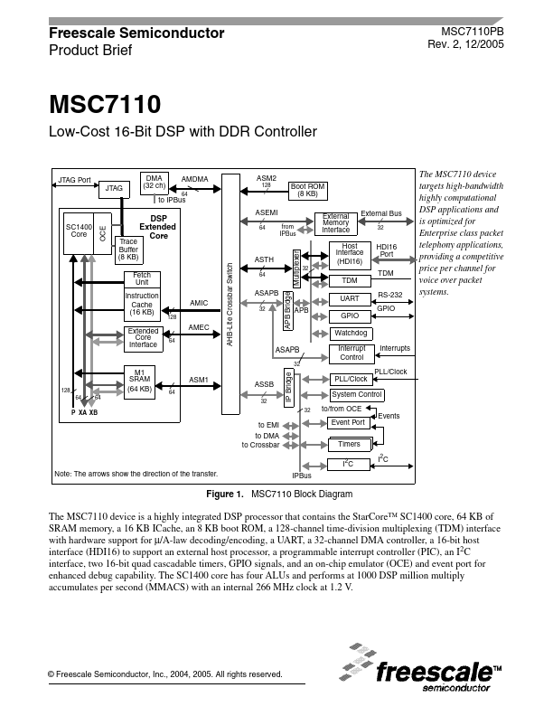
Datasheet Summary
Freescale Semiconductor Product Brief
MSC7110PB Rev. 2, 12/2005
Low-Cost 16-Bit DSP with DDR Controller
DMA (32 ch) ASM2
JTAG Port JTAG
AMDMA
Boot ROM (8 KB) External Memory Interface External Bus
32 to IPBus
SC1400 Core
AHB-Lite Crossbar Switch
ASTH
Multiplexer
Trace Buffer (8 KB)
DSP Extended Core
ASEMI
64 from IPBus
Host Interface (HDI16)
HDI16 Port TDM
Fetch Unit Instruction Cache (16 KB) Extended Core Interface AMIC
TDM UART RS-232 GPIO GPIO Watchdog
APB Bridge
ASAPB
The MSC7110 device targets high-bandwidth highly putational DSP applications and is optimized for Enterprise class packet telephony applications, providing a...