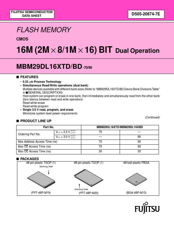
MBM29DL16xTD Description
) Host system can program or erase in one bank, then immediately and simultaneously read from the other bank Zero latency between read and write operations Read-while-erase Read-while-program Single 3.0 V read, program, and erase Minimizes system level power requirements (Continued) s PRODUCT LINE UP Part No. PFTN Normal Bend Type, PFTR Reversed Bend Type) 48-ball FBGA (Package suffix: PBT) Minimum 100,000...
MBM29DL16xTD Key Features
- 0.33 µm Process Technology
- Simultaneous Read/Write operations (dual bank) Multiple devices available with different bank sizes (Refer to “MBM29DL16
- Single 3.0 V read, program, and erase Minimizes system level power requirements (Continued)
- 70 70 30
- 90 90 90 35
- patible with JEDEC-standard mands Uses same software mands as E2PROMs
- patible with JEDEC-standard world-wide pinouts 48-pin TSOP(1) (Package suffix: PFTN
- Normal Bend Type, PFTR
- Reversed Bend Type) 48-ball FBGA (Package suffix: PBT)
- Minimum 100,000 program/erase cycles


