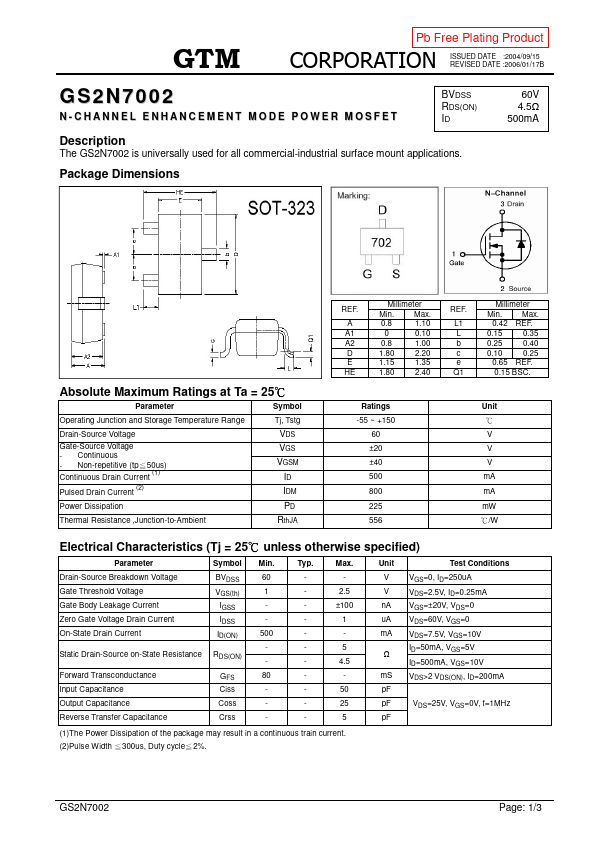
The following content is an automatically extracted verbatim text
from the original manufacturer datasheet and is provided for reference purposes only.
View original datasheet text
Pb Free Plating Product
ISSUED DATE :2004/09/15 REVISED DATE :2006/01/17B
GS2N7002
N-CHANNEL ENHANCEMENT MODE POWER MOSFET
BVDSS RDS(ON) ID
Description
The GS2N7002 is universally used for all commercial-industrial surface mount applications.
Package Dimensions
60V 4.5 500mA
Absolute Maximum Ratings at Ta = 25к
Parameter
Symbol
Operating Junction and Storage Temperature Range
Tj, Tstg
Drain-Source Voltage
Gate-Source Voltage - Continuous - Non-repetitive (tpЉ50us) Continuous Drain Current (1)
Pulsed Drain Current (2)
VDS VGS VGSM ID IDM
Power Dissipation
PD
Thermal Resistance ,Junction-to-Ambient
RthJA
REF.
A A1 A2 D E HE
Millimeter
Min. Max.
0.8
1.10
0
0.10
0.8
1.00
1.80
2.20
1.15
1.35
1.80
2.40
REF.
L1 L b c e Q1
Millimeter
Min. Max.
0.42 REF.
0.15
0.