HCD311 Key Features
- Please specify required code(s) when ordering
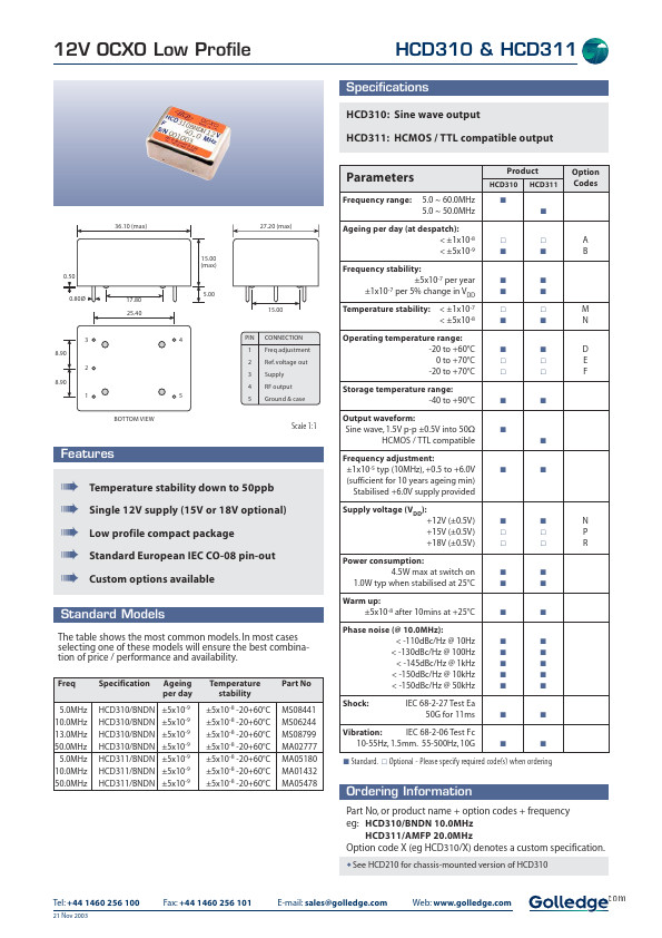
HCD311 is (HCD310 / HCD311) OCXO Low Profile manufactured by Golledge Electronics.
| Part Number | Description |
|---|---|
| HCD310 | (HCD310 / HCD311) OCXO Low Profile |
| HCD300 | OCXO |
| HCD301 | OCXO |
| HCD331 | OCXO HCMOS Low Profile |
| HCD332 | OCXO HCMOS OUTPUT STRATUM |
12V OCXO Low Profile HCD310 & HCD311 Specifications HCD310: HCMOS / TTL patible output Parameters Frequency range: < ±1x10⁻⁸ < ±5x10⁻⁹ Frequency stability:.