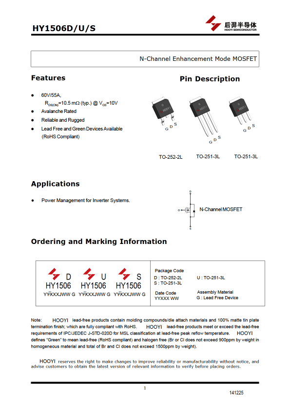
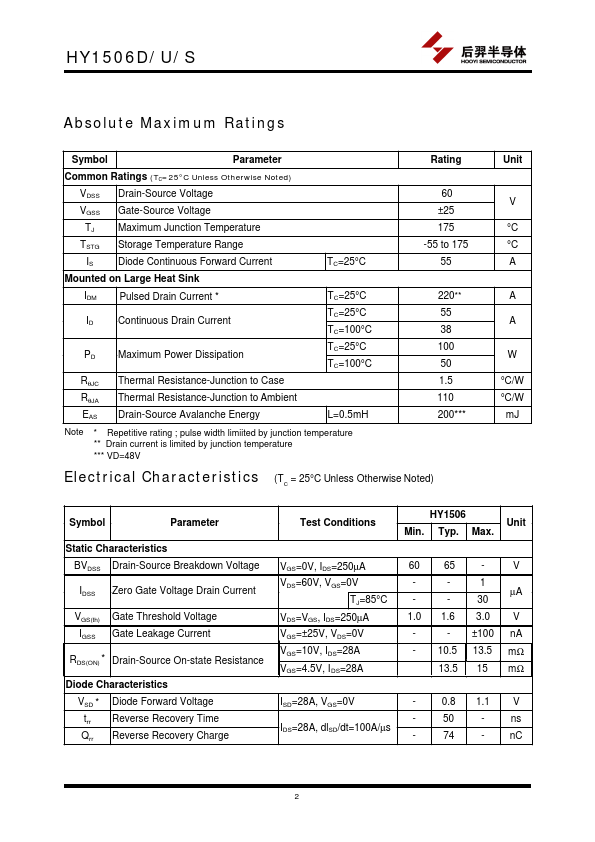
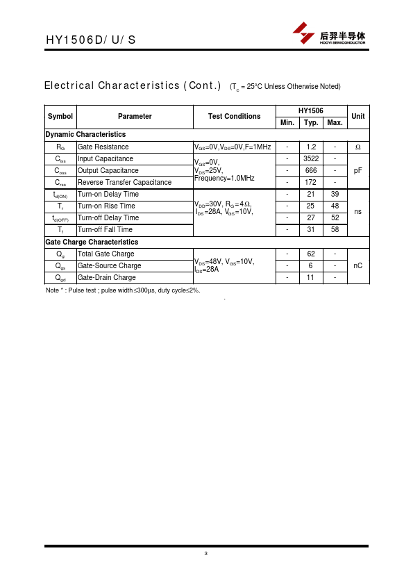
Download the HY1506S datasheet PDF.
This datasheet also covers the HY1506D variant, as both devices belong to the same n-channel mosfet family and are provided as variant models within a single manufacturer datasheet.
Full PDF Text Transcription for HY1506S (Reference)
Note: Below is a high-fidelity text extraction (approx. 800 characters) for
HY1506S. For precise diagrams, and layout, please refer to the original PDF.
HY1506D/U/S Absolute Maximum Ratings Symbol Parameter Common Ratings (TC=25°C Unless Otherwise Noted) VDSS Drain-Source Voltage VGSS Gate-Source Voltage TJ Maximum Juncti...
View more extracted text
) VDSS Drain-Source Voltage VGSS Gate-Source Voltage TJ Maximum Junction Temperature TSTG Storage Temperature Range IS Diode Continuous Forward Current Mounted on Large Heat Sink TC=25°C IDM Pulsed Drain Current * ID Continuous Drain Current PD Maximum Power Dissipation RθJC Thermal Resistance-Junction to Case RθJA Thermal Resistance-Junction to Ambient EAS Drain-Source Avalanche Energy TC=25°C TC=25°C TC=100°C TC=25°C TC=100°C L=0.5mH Note * Repetitive rating ; pulse width limiited by junction temperature ** Drain current is limited by junction temperature *** VD=48V Rating 60 ±25 175 -55 to 175 55 220** 55 38 100 50 1.