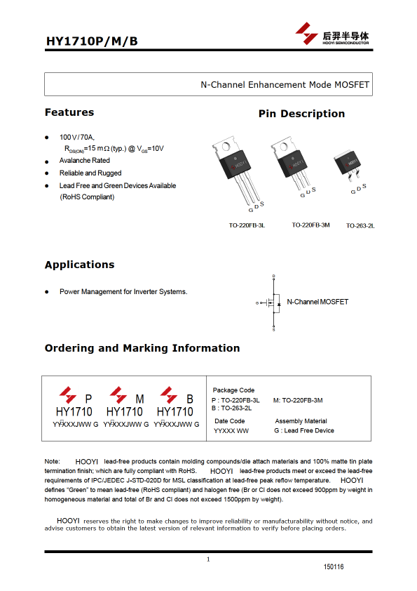
HY1710M Overview
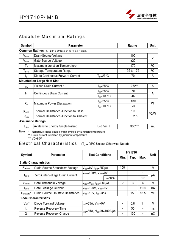
pulse width ≤300µs, duty cycle≤2%.
| Part number | HY1710M |
|---|---|
| Datasheet | HY1710M HY1710 Datasheet (PDF) |
| File Size | 562.58 KB |
| Manufacturer | HOOYI |
| Description | N-Channel MOSFET |
|
|
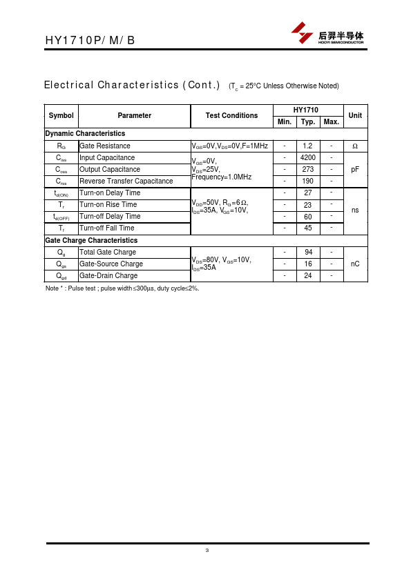
pulse width ≤300µs, duty cycle≤2%.
| Brand Logo | Part Number | Description | Manufacturer |
|---|---|---|---|
| HY1710B | Power MOSFET | VBsemi |