Download the CD4050B datasheet PDF.
This datasheet also covers the CD4049UB variant, as both devices belong to the same (cd4049ub / cd4050b) cmos hex buffer/converters family and are provided as variant models within a single manufacturer datasheet.
Key Features
CD4049UB Inverting.
CD4050B Non-Inverting.
High Sink Current for Driving 2 TTL Loads.
High-To-Low Level Logic Conversion.
100% Tested for Quiescent Current at 20V.
Maximum Input Current of 1µA at 18V Over Full Package Temperature Range; 100nA at 18V and 25oC.
5V, 10V and 15V Parametric Ratings
[ /Title (CD40 49UB, CD405 www. DataSheet4U. com 0B) The CD4049UB and CD4050B are designated as /Subreplacements for CD4009UB and CD4010B, res.
Full PDF Text Transcription for CD4050B (Reference)
Note: Below is a high-fidelity text extraction (approx. 800 characters) for
CD4050B. For precise diagrams, and layout, please refer to the original PDF.
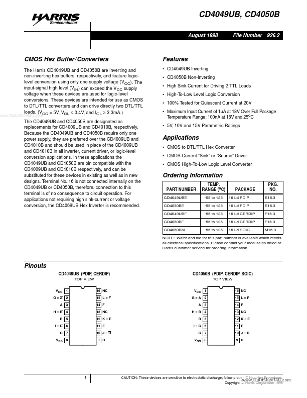
CD4049UB, CD4050B Semiconductor August 1998 File Number 926.2 CMOS Hex Buffer/Converters The Harris CD4049UB and CD4050B are inverting and non-inverting hex buffers, resp...
View more extracted text
CD4049UB and CD4050B are inverting and non-inverting hex buffers, respectively, and feature logiclevel conversion using only one supply voltage (VCC). The input-signal high level (VIH) can exceed the VCC supply voltage when these devices are used for logic-level conversions. These devices are intended for use as CMOS to DTL/TTL converters and can drive directly two DTL/TTL loads. (VCC = 5V, VOL ≤ 0.4V, and IOL ≥ 3.3mA.