CD4050BC
Description
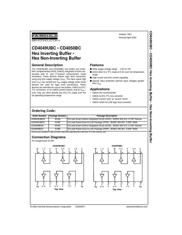
The CD4049UBC and CD4050BC hex buffers are monolithic complementary MOS (CMOS) integrated circuits constructed with N- and P-channel enhancement mode transistors. These devices feature logic level conversion using only one supply voltage (VDD).