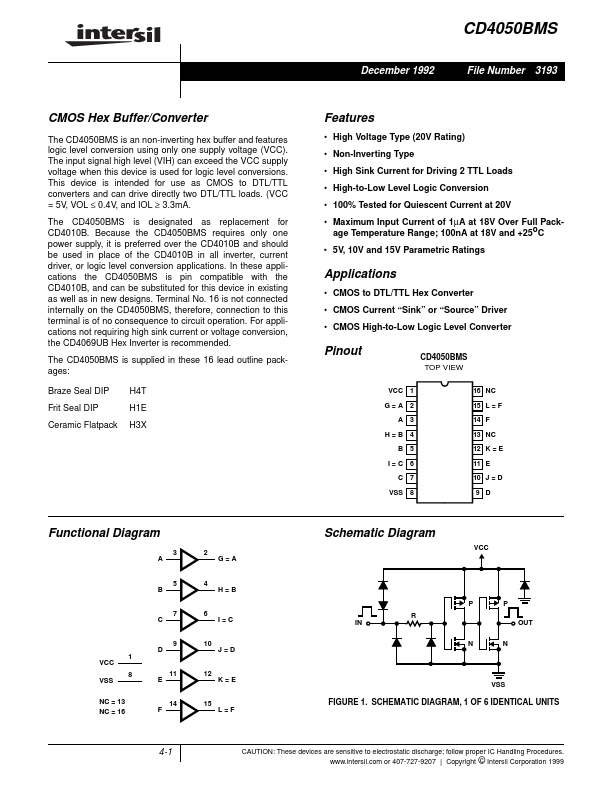
Datasheet4U Logo Datasheet4U.com

CD4050BMS - CMOS Hex Buffer/Converter

Key Features

  • logic level conversion using only one supply voltage (VCC). The input signal high level (VIH) can exceed the VCC supply voltage when this device is used for logic level conversions. This device is intended for use as CMOS to DTL/TTL converters and can drive directly two DTL/TTL loads. (VCC = 5V, VOL ≤ 0.4V, and IOL ≥ 3.3mA. The CD4050BMS is designated as replacement for CD4010B. Because the CD4050BMS requires only one power supply, it is preferred over the CD4010B and should be used in place of.

📥 Download Datasheet

Full PDF Text Transcription (Reference)

The following content is an automatically extracted verbatim text from the original manufacturer datasheet and is provided for reference purposes only.

View original datasheet text
CD4050BMS December 1992 File Number 3193 CMOS Hex Buffer/Converter The CD4050BMS is an non-inverting hex buffer and features logic level conversion using only one supply voltage (VCC). The input signal high level (VIH) can exceed the VCC supply voltage when this device is used for logic level conversions. This device is intended for use as CMOS to DTL/TTL converters and can drive directly two DTL/TTL loads. (VCC = 5V, VOL ≤ 0.4V, and IOL ≥ 3.3mA. The CD4050BMS is designated as replacement for CD4010B. Because the CD4050BMS requires only one power supply, it is preferred over the CD4010B and should be used in place of the CD4010B in all inverter, current driver, or logic level conversion applications.