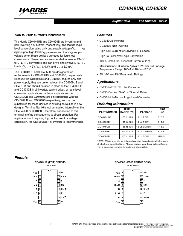
CD4050B
Key Features
- CD4049UB Inverting
- CD4050B Non-Inverting
- High Sink Current for Driving 2 TTL Loads
- High-To-Low Level Logic Conversion
- 100% Tested for Quiescent Current at 20V
- Maximum Input Current of 1µA at 18V Over Full Package Temperature Range; 100nA at 18V and 25oC
- 5V, 10V and 15V Parametric Ratings [ /Title (CD40 49UB, CD405 www.DataSheet4U.com 0B) The CD4049UB and CD4050B are designated as /Subreplacements for CD4009UB and CD4010B, respectively. Because the CD4049UB and CD4050B require only one ject (CMO power supply, they are preferred over the CD4009UB and S Hex CD4010B and should be used in place of the CD4009UB and CD4010B in all inverter, current driver, or logic-level Buffer/ conversion applications. In these applications the ConCD4049UB and CD4050B are pin compatible with the verters) CD4009UB and CD4010B respectively, and can be /Autho substituted for these devices in existing as well as in new designs. Terminal No. 16 is not connected internally on the r () CD4049UB or CD4050B, therefore, connection to this /Keyterminal is of no consequence to circuit operation. For words applications not requiring high sink-current or voltage (Harris conversion, the CD4069UB Hex Inverter is recommended. Semiconductor, CD400 0, metal gate, CMOS Pinouts