Datasheet Summary
..
Bus Buffer Gate with 3- state Output
ADE-205-333B (Z) 3rd. Edition April 2000 Description
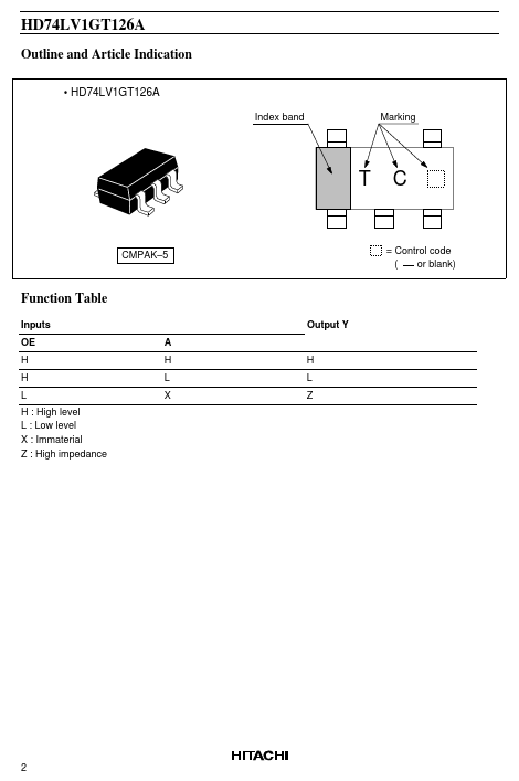
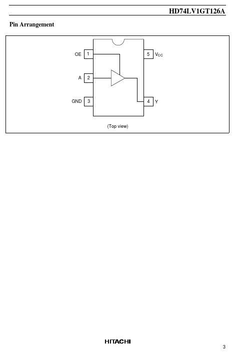
The HD74LV1GT126A has a bus buffer gate with 3- state output in a 5 pin package. Output is disabled when the associated output enable (OE) input is low. To ensure the high impedance state during power up or power down, OE should be connected to VCC through a pull-down resistor; the minimum value of the resistor is determined by the current souring capability of the driver. Low voltage and high speed operation is suitable for the battery powered products (e.g., notebook puters), and the low power consumption extends the battery life.
Features
- The basic gate...