Datasheet4U Logo Datasheet4U.com

HYMD564646CP8J - 184Pin Unbuffered DDR SDRAM DIMMs

Description

and is subject to change without notice.

Hynix Semiconductor does not assume any responsibility for use of circuits described.

No patent licenses are implied.

Features

  • JEDEC Standard 184-pin dual in-line memory module (DIMM) Two ranks 128M x 72, 128M x 64 and One rank 64M x 72, 64M x 64, 32M x 64 organization 2.6V ± 0.1V VDD and VDDQ Power supply for DDR400, 2.5V ± 0.2V for DDR333 and below All inputs and outputs are compatible with SSTL_2 interface Fully differential clock operations (CK & /CK) with 133/166/200MHz DLL aligns DQ and DQS transition with CK transition Programmable CAS Latency:.

📥 Download Datasheet

Full PDF Text Transcription (Reference)

The following content is an automatically extracted verbatim text from the original manufacturer datasheet and is provided for reference purposes only.

View original datasheet text
www.DataSheet4U.com 184pin Unbuffered DDR SDRAM DIMMs based on 512Mb C ver. (TSOP) 
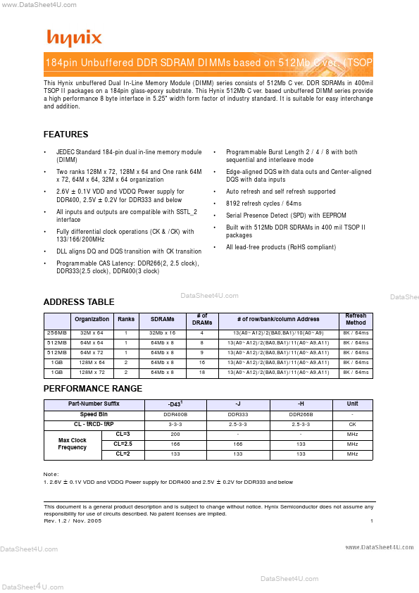
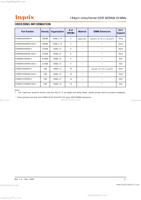
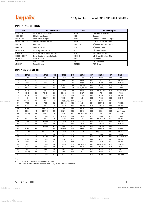
This Hynix unbuffered Dual In-Line Memory Module (DIMM) series consists of 512Mb C ver. DDR SDRAMs in 400mil TSOP II packages on a 184pin glass-epoxy substrate. This Hynix 512Mb C ver. based unbuffered DIMM series provide a high performance 8 byte interface in 5.25" width form factor of industry standard. It is suitable for easy interchange and addition. FEATURES • • • • • • • JEDEC Standard 184-pin dual in-line memory module (DIMM) Two ranks 128M x 72, 128M x 64 and One rank 64M x 72, 64M x 64, 32M x 64 organization 2.6V ± 0.1V VDD and VDDQ Power supply for DDR400, 2.5V ± 0.
Published: |