HY57V28820HCT-L Overview
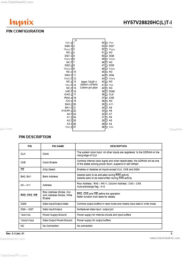
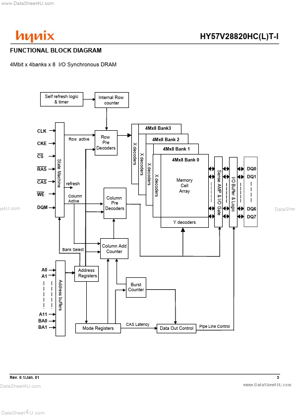
The Hynix HY57V28820HC(L)T is a 134,217,728bit CMOS Synchronous DRAM, ideally suited for the Mobile applications which require low power consumption and extended temperature range. f HY57V28820HC(L)T is organized as 4banks of 4,194,304x8. HY57V28820HC(L)T is offering fully synchronous operation referenced to a positive edge of the clock.
HY57V28820HCT-L Key Features
- Single 3.3±0.3V power supply All device pins are patible with LVTTL interface JEDEC standard 400mil 54pin TSOP-II with 0
- Auto refresh and self refresh 4096 refresh cycles / 64ms Programmable Burst Length and Burst Type
- 1, 2, 4, 8 or Full Page for Sequential Burst
- 1, 2, 4 or 8 for Interleave Burst