HY57V561620CT Description
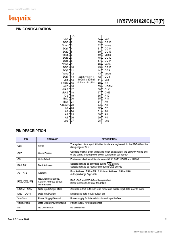
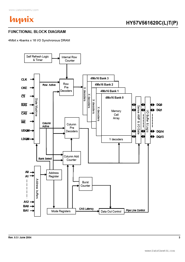
The HY57V561620C(L)T(P) Series is a 268,435,456bit CMOS Synchronous DRAM, ideally suited for the main memory applications which require large memory density and high bandwidth. HY57V561620C(L)T(P) Series is organized as 4banks of 4,194,304x16. HY57V561620C(L)T(P) Series is offering fully synchronous operation referenced to a positive edge of the clock.
HY57V561620CT Key Features
- Single 3.3±0.3V power supply All device pins are patible with LVTTL interface JEDEC standard 400mil 54pin TSOP-II with 0
- Auto refresh and self refresh 8192 refresh cycles / 64ms Programmable Burst Length and Burst Type
- 1, 2, 4, 8 or Full page for Sequential Burst
- 1, 2, 4 or 8 for Interleave Burst Programmable CAS Latency ; 2, 3 Clocks