ICS952623 Description
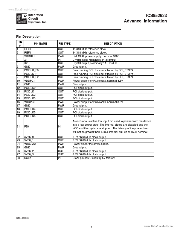
14.318 MHz reference clock. Ref, XTAL power supply, nominal 3.3V Crystal input,.
ICS952623 Key Features
- 0.7V current-mode differential CPU pairs
- 0.7V current-mode differential SRC pair
- PCI (33MHz)
- PCICLK_F, (33MHz) free-running
- USB, 48MHz
- DOT, 48MHz
- REF, 14.318MHz
- 3V66, 66.66MHz
- VCH/3V66, selectable 48MHz or 66MHz Key Specifications
- CPU/SRC outputs cycle-cycle jitter < 125ps