5PB1104PGG Overview
Key Specifications
Package: TSSOP
Mount Type: Surface Mount
Pins: 8
Operating Voltage: 1.8 V
Description
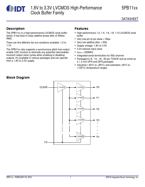
The 5PB11xx is a high-performance LVCMOS clock buffer family. It has best-in-class additive phase jitter of 50fsec RMS.
Key Features
- Very low pin-to-pin skew < 50ps
- Very low additive jitter < 50fs
- Supply voltage: 1.8V to 3.3V
- 3.3V tolerant input clock
- fMAX = 200MHz