ICS87008I
LOW SKEW, 1-TO-8
DIFFERENTIAL-TO-LVCMOS/LVTTL CLOCK GENERATOR
GENERAL DESCRIPTION
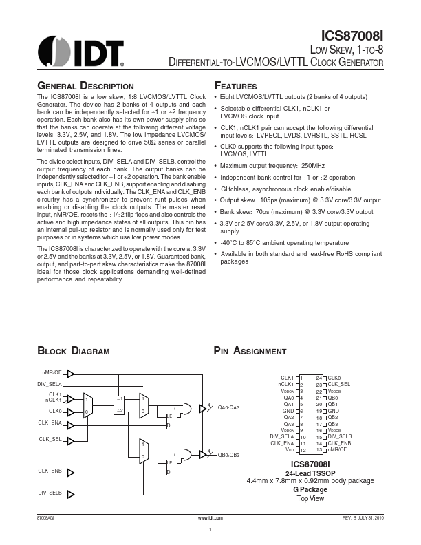
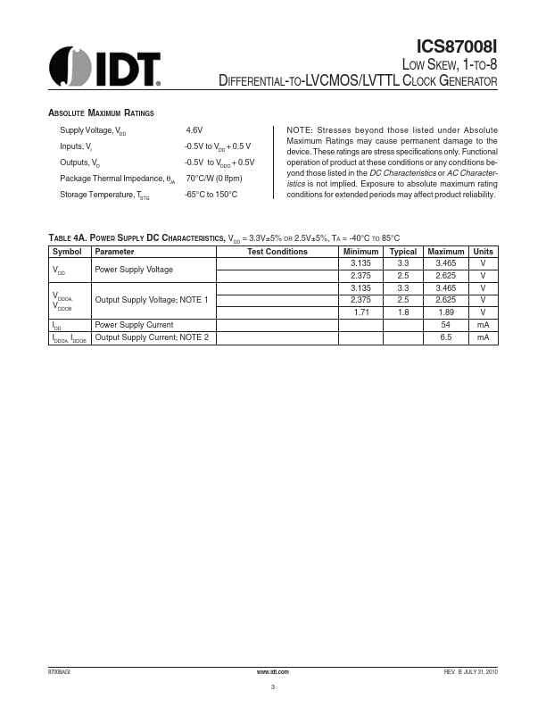
The ICS87008I is a low skew, 1:8 LVCMOS/LVTTL Clock
Generator. The device has 2 banks of 4 outputs and each
bank can be independently selected for ÷1 or ÷2 frequency
operation. Each bank also has its own power supply pins so
that the banks can operate at the following different voltage
levels: 3.3V, 2.5V, and 1.8V. The low impedance LVCMOS/
LVTTL outputs are designed to drive 50Ω series or parallel
terminated transmission lines.
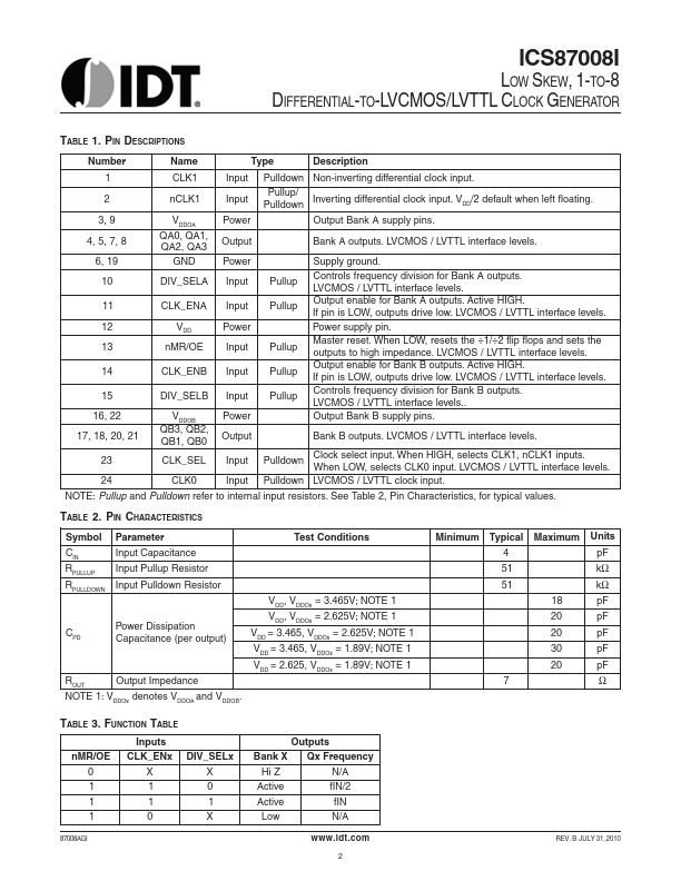
The divide select inputs, DIV_SELA and DIV_SELB, control the
output frequency of each bank. The output banks can be
independently selected for ÷1 or ÷2 operation. The bank enable
inputs, CLK_ENA and CLK_ENB, support enabling and disabling
each bank of outputs individually. The CLK_ENA and CLK_ENB
circuitry has a synchronizer to prevent runt pulses when
enabling or disabling the clock outputs. The master reset
input, nMR/OE, resets the ÷1/÷2 flip flops and also controls the
active and high impedance states of all outputs. This pin has
an internal pull-up resistor and is normally used only for test
purposes or in systems which use low power modes.
The ICS87008I is characterized to operate with the core at 3.3V
or 2.5V and the banks at 3.3V, 2.5V, or 1.8V. Guaranteed bank,
output, and part-to-part skew characteristics make the 87008I
ideal for those clock applications demanding well-defined
performance and repeatability.
FEATURES
• Eight LVCMOS/LVTTL outputs (2 banks of 4 outputs)
• Selectable differential CLK1, nCLK1 or
LVCMOS clock input
• CLK1, nCLK1 pair can accept the following differential
input levels: LVPECL, LVDS, LVHSTL, SSTL, HCSL
• CLK0 supports the following input types:
LVCMOS, LVTTL
• Maximum output frequency: 250MHz
• Independent bank control for ÷1 or ÷2 operation
• Glitchless, asynchronous clock enable/disable
• Output skew: 105ps (maximum) @ 3.3V core/3.3V output
• Bank skew: 70ps (maximum) @ 3.3V core/3.3V output
• 3.3V or 2.5V core/3.3V, 2.5V, or 1.8V output operating
supply
• -40°C to 85°C ambient operating temperature
• Available in both standard and lead-free RoHS compliant
packages
BLOCK DIAGRAM
nMR/OE
DIV_SELA
CLK1
nCLK1
CLK0
CLK_ENA
CLK_SEL
1
0
CLK_ENB
÷1 1
÷2 0
1
0
DIV_SELB
LE
D
LE
D
87008AGI
PIN ASSIGNMENT
4 QA0:QA3
4
QB0:QB3
CLK1
nCLK1
VDDOA
QA0
QA1
GND
QA2
QA3
VDDOA
DIV_SELA
CLK_ENA
VDD
1
2
3
4
5
6
7
8
9
10
11
12
24 CLK0
23 CLK_SEL
2 2 VDDOB
21 QB0
20 QB1
19 GND
18 QB2
17 QB3
1 6 VDDOB
15 DIV_SELB
14 CLK_ENB
13 nMR/OE
ICS87008I
24-Lead TSSOP
4.4mm x 7.8mm x 0.92mm body package
G Package
Top View
www.idt.com
1
REV. B JULY 31, 2010