IDT71V2577SA
Description
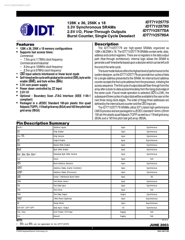
The IDT71V2577/79 are high-speed SRAMs organized as 128K x 36/256K x 18. The IDT71V2577/79 SRAMs contain write, data, address and control registers.
The IDT71V2577/79 are high-speed SRAMs organized as 128K x 36/256K x 18. The IDT71V2577/79 SRAMs contain write, data, address and control registers.