IDT72V261LA
IDT72V261LA is CMOS FIFO memories manufactured by IDT.
FEATURES
:
- Choose among the following memory organizations: IDT72V261LA
- 16,384 x 9 IDT72V271LA
- 32,768 x 9
- Pin-patible with the IDT72V281/72V291 and IDT72V2101/ 72V2111Super Sync FIFOs
- Functionally patible with the 5 Volt IDT72261/72271 family
- 10ns read/write cycle time (6.5ns access time)
- Fixed, low first word data latency time
- 5V input tolerant
- Auto power down minimizes standby power consumption
- Master Reset clears entire FIFO
- Partial Reset clears data, but retains programmable settings
- Retransmit operation with fixed, low first word data latency time
- Empty, Full and Half-Full flags signal FIFO status
- Programmable Almost-Empty and Almost-Full flags, each flag can default to one of two preselected offsets
- Program partial flags by either serial or parallel means
- Select IDT Standard timing (using EF and FF flags) or First
Word Fall Through timing (using OR and IR flags)
- Output enable puts data outputs into high impedance state
- Easily expandable in depth and width
- Independent Read and Write clocks (permit reading and writing simultaneously)
- Available in the 64-pin Thin Quad Flat Pack (TQFP) and the 64- pin Slim Thin Quad Flat Pack (STQFP)
- High-performance submicron CMOS technology
- Industrial temperature range (- 40°C to +85°C) is available
- Green parts available, see ordering information
DESCRIPTION
:
The IDT72V261LA/72V271LA are functionally patible versions of the IDT72261/72271 designed to run off a 3.3V supply for very low power consumption. The IDT72V261LA/72V271LA are exceptionally deep, high speed, CMOS First-In-First-Out (FIFO) memories with clocked read and
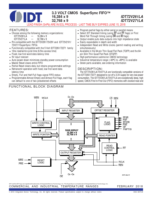
FUNCTIONAL BLOCK DIAGRAM
WEN WCLK
D0 -D8
LD SEN
WRITE CONTROL LOGIC
WRITE POINTER
INPUT REGISTER
RAM ARRAY 16,384 x 9 32,768 x 9
OFFSET REGISTER
FLAG LOGIC
READ...