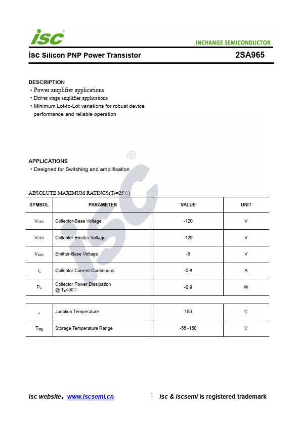
Power amplifier applications
Driver stage amplifier applications
Minimum Lot-to-Lot variations for robust device
performance and reliable operation
INCHANGE Semiconductor
2SA965
APPLICATIONS
Designed for Switching and amplification
ABSOLUTE MAXIMUM RATINGS(Ta=25℃)
SYMBOL
PAR
The following content is an automatically extracted verbatim text
from the original manufacturer datasheet and is provided for reference purposes only.
View original datasheet text
isc Silicon PNP Power Transistor
DESCRIPTION
·Power amplifier applications
·Driver stage amplifier applications ·Minimum Lot-to-Lot variations for robust device
performance and reliable operation
INCHANGE Semiconductor
2SA965
APPLICATIONS ·Designed for Switching and amplification
ABSOLUTE MAXIMUM RATINGS(Ta=25℃)
SYMBOL
PARAMETER
VCBO
Collector-Base Voltage
VCEO
Collector-Emitter Voltage
VEBO
Emitter-Base Voltage
IC
Collector Current-Continuous
PC
Collector Power Dissipation @ Ta<50℃
J
Junction Temperature
Tstg
Storage Temperature Range
VALUE -120 -120 -5 -0.8 -0.9
150 -55~150
UNIT V V V A W
℃ ℃
isc website:www.iscsemi.