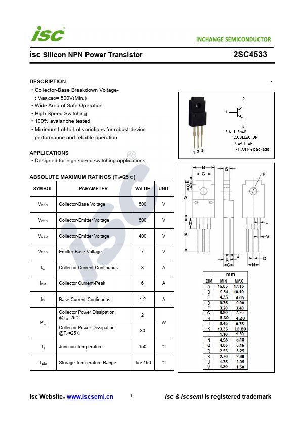
Collector-Base Breakdown Voltage-
: V(BR)CBO= 500V(Min.)
Wide Area of Safe Operation
High Speed Switching
100% avalanche tested
Minimum Lot-to-Lot variations for robust device
performance and reliable operation
APPLICATIONS
Designed for high speed switchi
The following content is an automatically extracted verbatim text
from the original manufacturer datasheet and is provided for reference purposes only.
View original datasheet text
isc Silicon NPN Power Transistor
INCHANGE Semiconductor
2SC4533
DESCRIPTION
·
·Collector-Base Breakdown Voltage-
: V(BR)CBO= 500V(Min.)
·Wide Area of Safe Operation
·High Speed Switching
·100% avalanche tested
·Minimum Lot-to-Lot variations for robust device
performance and reliable operation
APPLICATIONS ·Designed for high speed switching applications.
ABSOLUTE MAXIMUM RATINGS (Ta=25℃)
SYMBOL
PARAMETER
VALUE
UNIT
VCBO
Collector-Base Voltage
500
V
VCES
Collector-Emitter Voltage
500
V
VCEO
Collector-Emitter Voltage
400
V
VEBO
Emitter-Base Voltage
7
V
IC
Collector Current-Continuous
3
A
ICM
Collector Current-Peak
6
A
IB
Base Current-Continuous
Collector Power Dissipation @Ta=25℃
PC Collector Power Dissipation @TC=25℃
Tj
Junction Temperature
1.