FQU10N20 Overview
Key Specifications
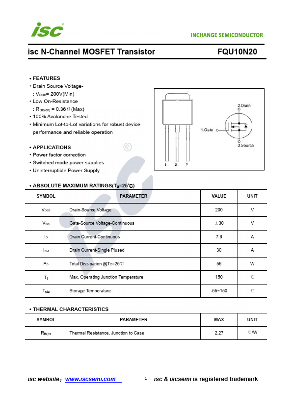
Package: TO-251-3
Mount Type: Through Hole
Pins: 3
Max Operating Temp: 150 °C
Key Features
- Drain Source Voltage- : VDSS= 200V(Min)
- Low On-Resistance : RDS(on) = 0.36Ω(Max)
- 100% Avalanche Tested
- Minimum Lot-to-Lot variations for robust device performance and reliable operation