IS49NLC36800A Overview
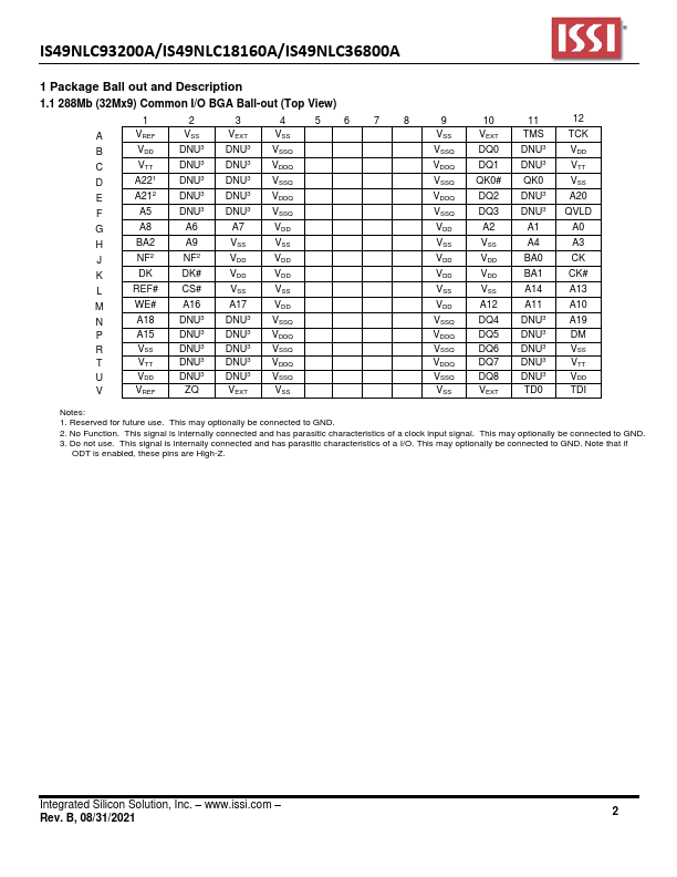
1.1 288Mb (32Mx9) mon I/O BGA Ball-out (Top View) 1 2 3 4 56 7 8 9 10 11 12 A VREF VSS VEXT VSS VSS VEXT TMS TCK B VDD DNU3 DNU3 VSSQ VSSQ DQ0 DNU3 VDD C VTT DNU3 DNU3 VDDQ VDDQ DQ1 DNU3 VTT D A221 DNU3 DNU3 VSSQ VSSQ QK0#.
IS49NLC36800A Key Features
- 533MHz DDR operation (1.067 Gb/s/pin data rate)
- 38.4Gb/s peak bandwidth (x36 at 533 MHz clock
- Reduced cycle time (15ns at 533MHz)
- 32ms refresh (8K refresh for each bank; 64K refresh
- 8 internal banks
- Non-multiplexed addresses (address multiplexing
- SRAM-type interface
- Programmable READ latency (RL), row cycle time
- Data mask signals (DM) to mask signal of WRITE
- Differential input clocks (CK, CK#)