CPC1390GRTR
CPC1390GRTR is 4-Pin OptoMOS Relay manufactured by IXYS.
- Part of the CPC1390 comparator family.
- Part of the CPC1390 comparator family.
INTEGRATED CIRCUITS DIVISION
Parameter Peak Blocking Voltage Load Current On-Resistance (max)
Rating 400 140 22
Units
VP mArms / mADC
Features
- 5000Vrms Input/Output Isolation
- 400VP Blocking Voltage
- 100% Solid State
- Low Drive Power Requirements
- Arc-Free With No Snubbing Circuits
- No EMI/RFI Generation
- Small 4-Pin Package
Applications
- Instrumentation
- Multiplexers
- Data Acquisition
- Electronic Switching
- I/O Subsystems
- Meters (Watt-Hour, Water, Gas)
- Medical Equipment- Patient/Equipment Isolation
- Security
- Aerospace
- Industrial Controls
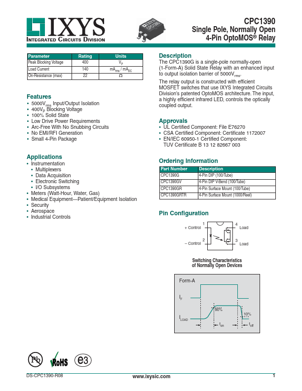
CPC1390
Single Pole, Normally Open
4-Pin OptoMOS® Relay
Description
The CPC1390G is a single-pole normally-open (1-Form-A)...