°C Ultra-low On Resistance
°C Unclamped Inductive Switching (UIS)
°C °C
rated Low package inductance - easy to drive and to protect
g 175 °C Operating Temperature
Symbol
Test Conditions
(TJ = 25°C unless otherwise specified)
BVDSS
VGS = 0 V, ID = 250 μA
VGS(th)
VDS = VGS, ID = 250 μA
IGSS VGS = ± 20 V, VDS = 0 V
IDSS
VDS = VDSS
VGS = 0 V
TJ = 150°C
RDS(on)
VGS = 10 V, ID = 25 A, Note 1
Characteristic Values Min. Typ. Max. 85 V
2.0 4.0 V
± 200 nA
5 μA 250 μA 4.0 5.0 mΩ
Advant.
Full PDF Text Transcription for IXTA200N085T7 (Reference)
Note: Below is a high-fidelity text extraction (approx. 800 characters) for
IXTA200N085T7. For precise diagrams, and layout, please refer to the original PDF.
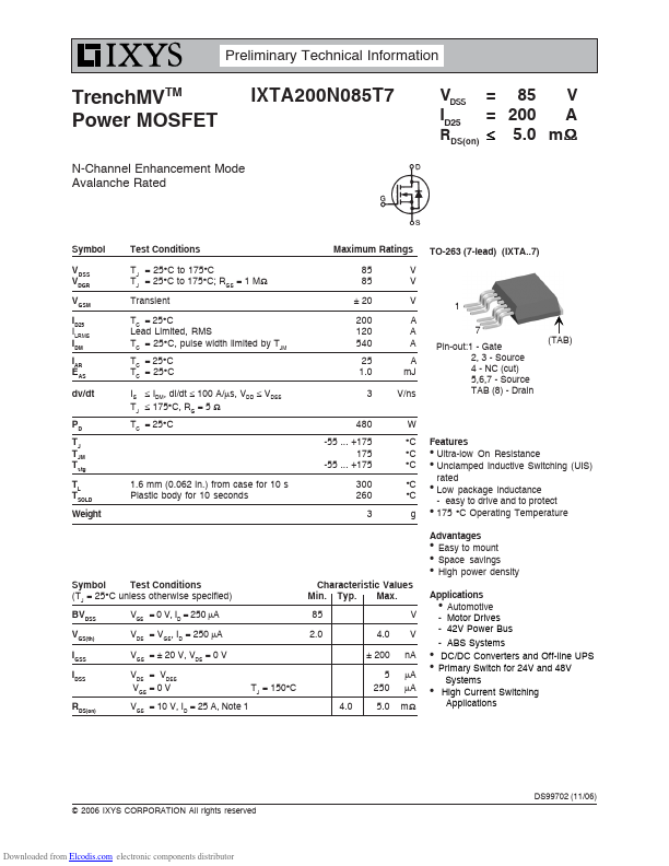
Preliminary Technical Information TrenchMVTM IXTA200N085T7 Power MOSFET N-Channel Enhancement Mode Avalanche Rated VDSS = ID25 = RDS(on) ≤ 85 200 5.0 V A mΩ Symbol Test C...
View more extracted text
valanche Rated VDSS = ID25 = RDS(on) ≤ 85 200 5.0 V A mΩ Symbol Test Conditions Maximum Ratings TO-263 (7-lead) (IXTA..7) VDSS VDGR VGSM ID25 IIDLRMMS IAR EAS dv/dt PD TJ TJM Tstg TL TSOLD Weight TJ = 25°C to 175°C TJ = 25°C to 175°C; RGS = 1 MΩ Transient TC = 25°C Lead Limited, RMS TC = 25°C, pulse width limited by TJM TC = 25°C TC = 25°C IS ≤ IDM, di/dt ≤ 100 A/μs, VDD ≤ VDSS TJ ≤ 175°C, RG = 5 Ω TC = 25°C 1.6 mm (0.062 in.) from case for 10 s Plastic body for 10 seconds 85 V 85 V ± 20 V 1 200 A 120 A 7 540 A Pin-out:1 - Gate (TAB) 25 A 1.0 mJ 2, 3 - Source 4 - NC (cut) 5,6,7 - Source 3 V/ns TAB (8) - Drain 480 -55 ... +