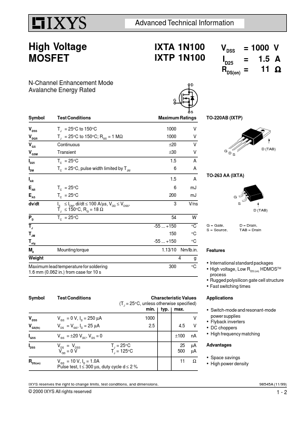
IXTP1N100
IXTP1N100 is High Voltage MOSFET manufactured by IXYS.
Features
Maximum lead temperature for soldering 1.6 mm (0.062 in.) from case for 10 s
International standard packages High voltage, Low RDS (on) HDMOSTM process
Rugged polysilicon gate cell structure Fast switching times
Symbol Test Conditions Characteristic Values (TJ = 25°C, unless otherwise specified) min. typ. max. 1000 2.5 4.5 ±100 TJ = 25°C TJ = 125°C 25 500 11 V V n A µA µA Ω Applications
Switch-mode and resonant-mode power supplies
VDSS VGS(th) IGSS IDSS RDS(on)
VGS = 0 V, ID = 250 µA VDS = VGS, ID = 25 µA VGS = ±20 VDC, VDS = 0 VDS = VDSS VGS = 0 V
Flyback inverters DC choppers High frequency matching
Advantages
VGS = 10 V, ID = 1.0A Pulse test, t ≤ 300 µs, duty cycle d ≤ 2 %
Space savings High power density
IXYS reserves the right to change limits, test conditions, and dimensions.
98545A (11/99)
© 2000 IXYS All rights reserved
1-2
IXTA 1N100 IXTP 1N100
Symbol Test Conditions Characteristic Values (TJ = 25°C, unless otherwise specified) min. typ. max. 0.8 1.5 480 VGS = 0 V, VDS = 25 V, f = 1 MHz 45 15 18 VGS = 10 V, VDS = 0.5
- VDSS, ID = 1A RG = 18Ω, (External) 19 20 18 23 VGS = 10 V, VDS = 0.5
- VDSS, ID = 1A 4.5 14 2.3 (IXTP) 0.50 S p F p F p F ns ns ns ns
Dim. Millimeter Min. Max. 4.06 2.03 0.51 1.14 0.46 1.14 8.64 7.11 9.65 6.86 2.54 14.61 2.29 1.02 1.27 0 0.46 4.83 2.79 0.99 1.40 0.74 1.40 9.65 8.13 10.29 8.13 BSC 15.88 2.79 1.40 1.78 0.38 0.74 Inches Min. Max. .160 .080 .020 .045 .018 .045 .340 .280 .380 .270 .100 .575 .090 .040 .050 0 .018 .190 .110 .039 .055 .029 .055 .380 .320 .405 .320 BSC .625 .110 .055 .070 .015 .029
TO-263 AA (IXTA) Outline gfs C iss Coss C rss td(on) tr td(off) tf Qg(on) Qgs Qgd Rth JC Rth CK
VDS = 20 V; ID = 1.0A, pulse test n C n C n C K/W K/W
A A1 b b2 c c2 D D1 E E1 e
Source-Drain Diode Symbol IS ISM VSD t rr Test Conditions VGS = 0 V
Characteristic Values (TJ = 25°C, unless otherwise specified) min. typ. max. 1.5 6 1.8 710 A A V ns
L L1 L2 L3 L4 R
Repetitive; pulse width limited by TJM...